- 您現(xiàn)在的位置:買賣IC網(wǎng) > PDF目錄98080 > SII3114CT176 PCI BUS CONTROLLER, PQFP176 PDF資料下載
參數(shù)資料
| 型號(hào): | SII3114CT176 |
| 元件分類: | 總線控制器 |
| 英文描述: | PCI BUS CONTROLLER, PQFP176 |
| 封裝: | TQFP-176 |
| 文件頁數(shù): | 90/127頁 |
| 文件大?。?/td> | 564K |
| 代理商: | SII3114CT176 |
第1頁第2頁第3頁第4頁第5頁第6頁第7頁第8頁第9頁第10頁第11頁第12頁第13頁第14頁第15頁第16頁第17頁第18頁第19頁第20頁第21頁第22頁第23頁第24頁第25頁第26頁第27頁第28頁第29頁第30頁第31頁第32頁第33頁第34頁第35頁第36頁第37頁第38頁第39頁第40頁第41頁第42頁第43頁第44頁第45頁第46頁第47頁第48頁第49頁第50頁第51頁第52頁第53頁第54頁第55頁第56頁第57頁第58頁第59頁第60頁第61頁第62頁第63頁第64頁第65頁第66頁第67頁第68頁第69頁第70頁第71頁第72頁第73頁第74頁第75頁第76頁第77頁第78頁第79頁第80頁第81頁第82頁第83頁第84頁第85頁第86頁第87頁第88頁第89頁當(dāng)前第90頁第91頁第92頁第93頁第94頁第95頁第96頁第97頁第98頁第99頁第100頁第101頁第102頁第103頁第104頁第105頁第106頁第107頁第108頁第109頁第110頁第111頁第112頁第113頁第114頁第115頁第116頁第117頁第118頁第119頁第120頁第121頁第122頁第123頁第124頁第125頁第126頁第127頁
SiI3114 PCI to Serial ATA Controller
Data Sheet
Silicon Image, Inc.
2007 Silicon Image, Inc.
57
SiI-DS-0103-D
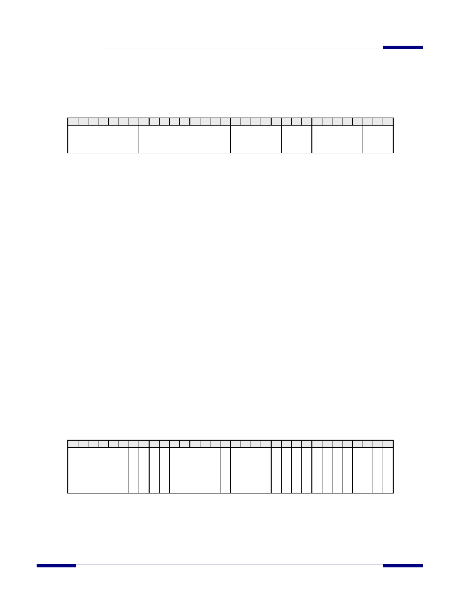
FIFO Valid Byte Count and Control – Channel X
Address Offset: 40H / 44H / 240H / 244H
Access Type: Read/Write
Reset Value: 0x0000_0000
31 30 29 28 27 26 25 24 23 22 21 20 19 18 17 16 15 14 13 12 11 10 09 08 07 06 05 04 03 02 01 00
Reserved
FIFO Valid Byte Count
Reserved
FIFO Wr
Req Ctrl
Reserved
FIFO Rd
Req Ctrl
This register defines the FIFO valid byte count register and PCI bus request control for Channel X in the SiI3114.
The register bits are defined below.
The FIFO Write Request Control and FIFO Read Request Control fields in these registers provide threshold
settings for establishing when PCI requests are made to the Arbiter. The Arbiter arbitrates among the four
requests using fixed priority with masking. The fixed priority is, from highest to lowest: channel 0; channel 1;
channel 2; and channel 3. If multiple requests are present, the arbiter grants PCI bus access to the highest
priority channel that is not masked. That channel’s request is then masked as long as any unmasked requests are
present.
Bit [31:25]: Reserved (R). This bit field is reserved and returns zeros on a read.
Bit [24:16]: FIFO Valid Byte Count (R). This bit field provides the valid byte count for the data FIFO for
Channel X. A value of 000H indicates empty, while a value of 100H indicates a full FIFO with 256 bytes.
Bit [15:11]: Reserved (R). This bit field is reserved and returns zeros on a read.
Bit [10:08]: FIFO Wr Req Ctrl (R/W) – FIFO Write Request Control. This bit field defines the FIFO
threshold to assign priority when requesting a PCI bus write operation. A value of 00H indicates that write
request priority is set whenever the FIFO contains greater than 32 bytes, while a value of 07H indicates that
write request priority is set whenever the FIFO contains greater than 7x32 bytes (=224 bytes). This bit field
is useful when multiple DMA channels are competing for the PCI bus.
Bit [07:03]: Reserved (R). This bit field is reserved and returns zeros on a read.
Bit [02:00]: FIFO Rd Req Ctrl (R/W) – FIFO Read Request Control. This bit field defines the FIFO
threshold to assign priority when requesting a PCI bus read operation. A value of 00H indicates that read
request priority is set whenever the FIFO has greater than 32 bytes available space, while a value of 07H
indicates that read request priority is set whenever the FIFO has greater than 7x32 bytes (=224 bytes)
available space. This bit field is useful when multiple DMA channels are competing for accessing the PCI
bus.
System Configuration Status – Command
Address Offset: 48H
Access Type: Read/Write
Reset Value: 0x0000_0000
31 30 29 28 27 26 25 24 23 22 21 20 19 18 17 16 15 14 13 12 11 10 09 08 07 06 05 04 03 02 01 00
Reserved
C
hnl3
Int
B
lock
C
hnl2
Int
B
lock
C
hnl1
Int
B
lock
C
hnl0
Int
B
lock
Reserved
M
66EN
Reserved
Chnl2
Module
Rst
Chnl3
Module
Rst
FF2
Module
Rst
FF3
Module
Rst
Chnl0
Module
Rst
Chnl1
Module
Rst
FF0
Module
Rst
FF1
Module
Rst
R
eserved
ARB
Module
Rs
t
PBM
Module
Rst
This register defines the system configuration status and command register for the SiI3114. The register bits are
defined below.
Bit [31:26]: Reserved (R). This bit field is reserved and returns zeros on a read.
Bit [25]: Chnl3 Int Block (R/W) – Channel3 Interrupt Block. This bit is set to block interrupts from Channel
3.
相關(guān)PDF資料 |
PDF描述 |
|---|---|
| SII3114CTU | PCI BUS CONTROLLER, PQFP176 |
| SII3124ACBHU | PCI BUS CONTROLLER, PBGA364 |
| SII3512ECTU128 | PCI BUS CONTROLLER, PQFP128 |
| SII3531ACNU | PCI BUS CONTROLLER, QCC48 |
| SIO10N268-NU | MULTIFUNCTION PERIPHERAL, PQFP128 |
相關(guān)代理商/技術(shù)參數(shù) |
參數(shù)描述 |
|---|---|
| SII3114CTU | 制造商:Silicon Image Inc 功能描述:PCI to Serial ATA Controller 176-Pin TQFP 制造商:SILICON 功能描述: |
| SII3124A | 制造商:SILICONIMAGE 制造商全稱:SILICONIMAGE 功能描述:PCI-X to Serial ATA Controller |
| SII3124ACBHU | 制造商:SILICONIMAGE 制造商全稱:SILICONIMAGE 功能描述:PCI-X to Serial ATA Controller |
| SII3132 | 制造商:SILICONIMAGE 制造商全稱:SILICONIMAGE 功能描述:PCI Express to 2-Port Serial ATA II Host Controller |
| SII3132CNU | 制造商:Silicon Image Inc 功能描述:PCI Express to Serial ATA Controller 88-Pin QFN |
發(fā)布緊急采購,3分鐘左右您將得到回復(fù)。