- 您現(xiàn)在的位置:買賣IC網(wǎng) > PDF目錄385819 > SC28L92 (NXP Semiconductors N.V.) 3.3V- 5.0V Dual universal asynchronous receiver/transmitter (DUART)(3.3V- 5.0V雙通用異步接收器/傳送器) PDF資料下載
參數(shù)資料
| 型號: | SC28L92 |
| 廠商: | NXP Semiconductors N.V. |
| 英文描述: | 3.3V- 5.0V Dual universal asynchronous receiver/transmitter (DUART)(3.3V- 5.0V雙通用異步接收器/傳送器) |
| 中文描述: | 3.3 - 5.0V雙路通用異步接收/發(fā)送器(杜阿爾特)(3.3 - 5.0V雙通用異步接收器/傳送器) |
| 文件頁數(shù): | 8/44頁 |
| 文件大小: | 284K |
| 代理商: | SC28L92 |
第1頁第2頁第3頁第4頁第5頁第6頁第7頁當(dāng)前第8頁第9頁第10頁第11頁第12頁第13頁第14頁第15頁第16頁第17頁第18頁第19頁第20頁第21頁第22頁第23頁第24頁第25頁第26頁第27頁第28頁第29頁第30頁第31頁第32頁第33頁第34頁第35頁第36頁第37頁第38頁第39頁第40頁第41頁第42頁第43頁第44頁
Philips Semiconductors
Product specification
SC28L92
3.3V–5.0V Dual Universal Asynchronous
Receiver/Transmitter (DUART)
2000 Jan 21
8
)
áááááááááááááááááááááááááááááááááá
á
áááááááááááááááááááááááááááááááá
á
áááááááááááááááááááááááááááááááááá
á
áááááááááááááááááááááááááááááááá
áááááááááááááááááááááááááááááááááá
á
áááááááááááááááááááááááááááááááááá
á
áááááááááááááááááááááááááááááááááá
áááááááááááááááááááááááááááááááááá
á
áááá
á
áááááááááááááááááááááááááááááááááá
á
áááááááááááááááááááááááááááááááááá
áááááááááááááááááááááááááááááááááá
á
áááá
áááááááááááááááááááááááááááááááááá
áááááááááááááááááááááááááááááááááá
áááááááááááááááááááááááááááááááááá
á
áááááááááááááááááááááááááááááááááá
á
áááááááááááááááááááááááááááááááá
áááááááááááááááááááááááááááááááááá
áá
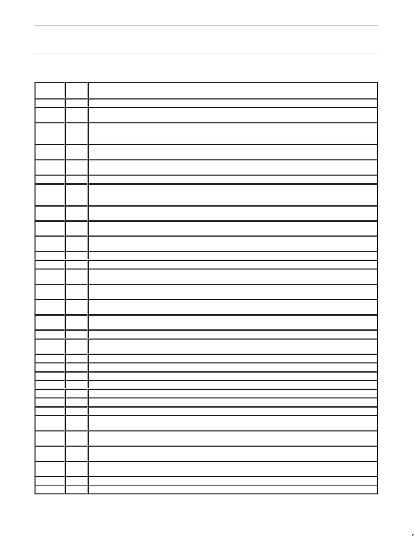
D0–D7
á
I/O
á
PIN
Data Bus
: Bi-directional 3-State data bus used to transfer commands, data and status between the DUART and the
Chip Enable
: Active-Low input signal. When Low, data transfers between the CPU and the DUART are enabled on
D0–D7 as controlled by the WRN, RDN and A0–A3 inputs. When High, places the D0–D7 lines in the 3-State
condition.
ááááááááááááááááááááááááááá
áááááááááááááááááááááááááááááááááá
áááááááááááááááááááááááááááááááááá
áá
áá
transfer occurs on the rising edge of the signal.
RDN
I
Read Strobe
: When Low and CEN is also Low, causes the contents of the addressed register to be presented on the
data bus. The read cycle begins on the falling edge of RDN.
stops the counter/timer, and puts Channels A and B in the inactive state, with the TxDA and TxDB outputs in the mark
á
á
á
áááááááááááááááááááááááááááááááááá
áá
interrupting conditions are true. This pin requires a pullup device.
X1/CLK
I
Crystal 1
: Crystal or external clock input. A crystal or clock of the specified limits must be supplied at all times. When a
to ground (see Figure 11). If X1/CLK is driven from an external source, this pin
must
be left open.
RxDA
I
Channel A Receiver Serial Data Input
: The least significant bit is received first. “Mark” is High; “space” is Low.
RxDB
I
Channel B Receiver Serial Data Input
: The least significant bit is received first. “Mark” is High; “space” is Low.
Channel A Transmitter Serial Data Output
: The least significant bit is transmitted first. This output is held in the “mark”
condition when the transmitter is disabled, idle or when operating in local loop back mode. “Mark” is High; “space” is Low.
TxDB
O
Channel B Transmitter Serial Data Output
: The least significant bit is transmitted first. This output is held in the ‘mark’
Output 0
: General purpose output or Channel A request to send (RTSAN, active-Low). Can be deactivated
automatically on receive or transmit.
OP1
O
Output 1
: General-purpose output or Channel B request to send (RTSBN, active-Low). Can be deactivated
output, or Channel B receiver 1X clock output.
OP4
O
Output 4
: General purpose output or Channel A open-drain, active-Low, RxA interrupt ISR[1] output.
IP1
I
Input 1
: General purpose input or Channel B clear to send active-Low input (CTSBN).
IP2
I
Input 2
: General-purpose input or counter/timer external clock input.
IP3
I
Input 3
: General purpose input or Channel A transmitter external clock input (TxCA). When the external clock is used
by the transmitter, the transmitted data is clocked on the falling edge of the clock.
the receiver, the received data is sampled on the rising edge of the clock.
Input 5
: General purpose input or Channel B transmitter external clock input (TxCB). When the external clock is used
by the transmitter, the transmitted data is clocked on the falling edge of the clock.
the receiver, the received data is sampled on the rising edge of the clock.
CC
á
á
áá
áááááááááááááááááááááááááááááááááá
áá
áááááááááááááááááááááááááááááááááá
áá
áááááááááááááááááááááááááááááááááá
áá
áááááááááááááááááááááááááááááááááá
áááááááááááááááááááááááááááááááááá
áá
áááááááááááááááááááááááááááááááááá
áá
áááááááááááááááááááááááááááááááááá
áááááááááááááááááááááááááááááááááá
á
á
á
á
á
á
á
á
á
á
á
á
Write Strobe
: When Low and CEN is also Low, the contents of the data bus is loaded into the addressed register. The
á
á
á
á
INTRN
á
á
á
Interrupt Request
: Active-Low, open-drain, output which signals the CPU that one or more of the eight maskable
á
á
á
á
á
á
á
á
á
á
á
á
á
á
á
á
á
相關(guān)PDF資料 |
PDF描述 |
|---|---|
| SC3011B-1 | 600.0 MHz Differential Sine-Wave Clock |
| SC3015B | 550.0 MHz Differential Sine-Wave Clock |
| SC3017B | 400.0 MHz Differential Sine-Wave Clock |
| sc3018b | Quartz SAW Frequency Stability |
| SC3019B | 500.0 MHz Differential Sine-Wave Clock |
相關(guān)代理商/技術(shù)參數(shù) |
參數(shù)描述 |
|---|---|
| SC28L92A1A | 制造商:NXP Semiconductors 功能描述:UART DUAL 3.3V OR 5V SMD 28L92 |
| SC28L92A1A,512 | 功能描述:UART 接口集成電路 3V-5V 2CH UART INTEL/MOT INTRF RoHS:否 制造商:Texas Instruments 通道數(shù)量:2 數(shù)據(jù)速率:3 Mbps 電源電壓-最大:3.6 V 電源電壓-最小:2.7 V 電源電流:20 mA 最大工作溫度:+ 85 C 最小工作溫度:- 40 C 封裝 / 箱體:LQFP-48 封裝:Reel |
| SC28L92A1A,518 | 功能描述:UART 接口集成電路 3V-5V 2CH UART RoHS:否 制造商:Texas Instruments 通道數(shù)量:2 數(shù)據(jù)速率:3 Mbps 電源電壓-最大:3.6 V 電源電壓-最小:2.7 V 電源電流:20 mA 最大工作溫度:+ 85 C 最小工作溫度:- 40 C 封裝 / 箱體:LQFP-48 封裝:Reel |
| SC28L92A1A,529 | 功能描述:UART 接口集成電路 3V-5V 2CH UART RoHS:否 制造商:Texas Instruments 通道數(shù)量:2 數(shù)據(jù)速率:3 Mbps 電源電壓-最大:3.6 V 電源電壓-最小:2.7 V 電源電流:20 mA 最大工作溫度:+ 85 C 最小工作溫度:- 40 C 封裝 / 箱體:LQFP-48 封裝:Reel |
| SC28L92A1A512 | 制造商:NXP Semiconductors 功能描述:IC DUAL UART FIFO 1MBPS 5.5V LCC-44 |
發(fā)布緊急采購,3分鐘左右您將得到回復(fù)。