- 您現(xiàn)在的位置:買賣IC網(wǎng) > PDF目錄98068 > S1C62740D 4-BIT, MROM, 1.3 MHz, MICROCONTROLLER, UUC109 PDF資料下載
參數(shù)資料
| 型號(hào): | S1C62740D |
| 元件分類: | 微控制器/微處理器 |
| 英文描述: | 4-BIT, MROM, 1.3 MHz, MICROCONTROLLER, UUC109 |
| 封裝: | DIE-109 |
| 文件頁數(shù): | 90/249頁 |
| 文件大?。?/td> | 1712K |
| 代理商: | S1C62740D |
第1頁第2頁第3頁第4頁第5頁第6頁第7頁第8頁第9頁第10頁第11頁第12頁第13頁第14頁第15頁第16頁第17頁第18頁第19頁第20頁第21頁第22頁第23頁第24頁第25頁第26頁第27頁第28頁第29頁第30頁第31頁第32頁第33頁第34頁第35頁第36頁第37頁第38頁第39頁第40頁第41頁第42頁第43頁第44頁第45頁第46頁第47頁第48頁第49頁第50頁第51頁第52頁第53頁第54頁第55頁第56頁第57頁第58頁第59頁第60頁第61頁第62頁第63頁第64頁第65頁第66頁第67頁第68頁第69頁第70頁第71頁第72頁第73頁第74頁第75頁第76頁第77頁第78頁第79頁第80頁第81頁第82頁第83頁第84頁第85頁第86頁第87頁第88頁第89頁當(dāng)前第90頁第91頁第92頁第93頁第94頁第95頁第96頁第97頁第98頁第99頁第100頁第101頁第102頁第103頁第104頁第105頁第106頁第107頁第108頁第109頁第110頁第111頁第112頁第113頁第114頁第115頁第116頁第117頁第118頁第119頁第120頁第121頁第122頁第123頁第124頁第125頁第126頁第127頁第128頁第129頁第130頁第131頁第132頁第133頁第134頁第135頁第136頁第137頁第138頁第139頁第140頁第141頁第142頁第143頁第144頁第145頁第146頁第147頁第148頁第149頁第150頁第151頁第152頁第153頁第154頁第155頁第156頁第157頁第158頁第159頁第160頁第161頁第162頁第163頁第164頁第165頁第166頁第167頁第168頁第169頁第170頁第171頁第172頁第173頁第174頁第175頁第176頁第177頁第178頁第179頁第180頁第181頁第182頁第183頁第184頁第185頁第186頁第187頁第188頁第189頁第190頁第191頁第192頁第193頁第194頁第195頁第196頁第197頁第198頁第199頁第200頁第201頁第202頁第203頁第204頁第205頁第206頁第207頁第208頁第209頁第210頁第211頁第212頁第213頁第214頁第215頁第216頁第217頁第218頁第219頁第220頁第221頁第222頁第223頁第224頁第225頁第226頁第227頁第228頁第229頁第230頁第231頁第232頁第233頁第234頁第235頁第236頁第237頁第238頁第239頁第240頁第241頁第242頁第243頁第244頁第245頁第246頁第247頁第248頁第249頁
I-6
EPSON
S1C62740 TECHNICAL HARDWARE
CHAPTER 1: OVERVIEW
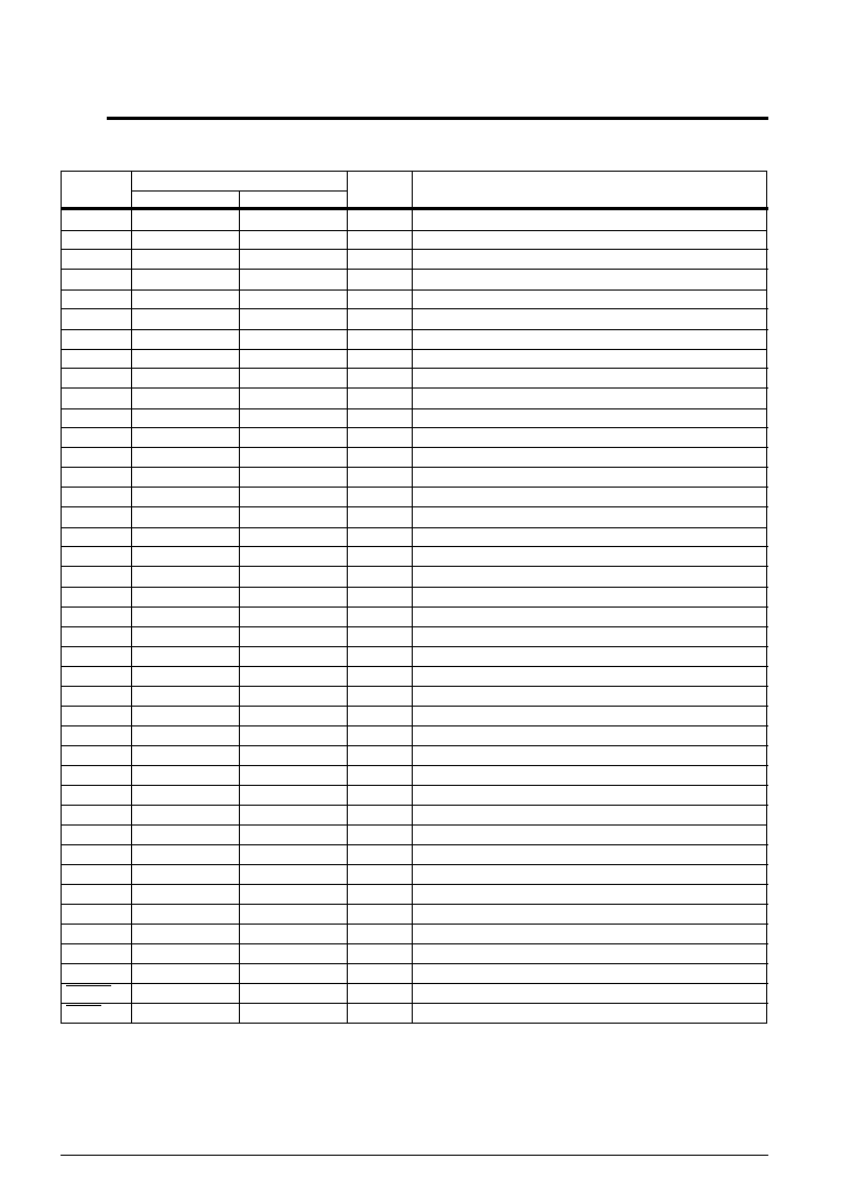
1.4 Pin Description
Table 1.4.1 Pin description
Pin name
Pin No.
QFP5-100pin
QFP15-100pin
In/Out
Function
11
6
88
78
87
98
35
34
33
36
32–30
7
8
9
10
3–1, 100, 99
16–23
24–27
15–12
40–37
41–72
80, 79, 77–75
74
82
81
84
83
73
85
86
95
96
97
90
91
89
92
93
94
28
29
9
4
86
76
85
96
33
32
31
34
30–28
5
6
7
8
1, 100–97
14–21
22–25
13–10
38–35
39–70
78, 77, 75–73
72
80
79
82
81
71
83
84
93
94
95
88
89
87
90
91
92
26
27
VDD
VSS
VDDA
VSSA
GND
VD1
VC1
VC2
VC3
VCA
CA–CC
OSC1
OSC2
OSC3
OSC4
K00–10
P00–13
P20–23
R00–03
COM0–3
SEG0–31
AI0–4
AIF
CAZ
CI
RI
BF
CO
CH
CL
VR1
VR2
VRA
AIP0
AIM0
AOUT0
AIP1
AIM1
AOUT1
RESET
TEST
(I)
(I/O)
–
I
O
I
O
I
I/O
O
I
–
(I)
–
I
O
I
O
I
Power (+)
Power (-)
Analog system power (+)
Analog system power (-)
Analog system ground
Internal logic system regulated voltage output
LCD system regulated voltage output
LCD system booster voltage output (VC1
× 2)
LCD system booster voltage output (VC1
× 3)
LCD system voltage adjustment pin
LCD system voltage booster condenser connecting pin
Crystal oscillator input
Crystal oscillator output
Ceramic or CR oscillator input (selected by mask option)
Ceramic or CR oscillator output (selected by mask option)
Input port
I/O port
I/O port or serial interface I/O pin (selected by software)
Output port (buzzer and clock outputs are selected by software)
LCD common output (1/4, 1/3, 1/2, 1/1 duty, programmable)
LCD segment output (DC output is selected by mask option)
Analog input
Analog input filter condenser connecting pin
Auto zero adjustment condenser connecting pin
Integral condenser connecting pin
Integral resistance connecting pin
Buffer amplifier output
Testing output pin
Reference voltage control condenser connecting pin
Reference voltage for resistance measurement
Reference voltage for voltage measurement
Reference voltage adjustment pin
AMP 0 non inverted input
AMP 0 inverted input
AMP 0 output
AMP 1 non inverted input
AMP 1 inverted input
AMP 1 output
System reset input pin
Testing input pin
相關(guān)PDF資料 |
PDF描述 |
|---|---|
| S1C62920D | 4-BIT, MROM, 1.3 MHz, MICROCONTROLLER, UUC63 |
| S1C62A33D | 4-BIT, MROM, 0.6 MHz, MICROCONTROLLER, UUC86 |
| S1C62N82F | 4-BIT, MROM, 0.032 MHz, MICROCONTROLLER, PQFP80 |
| S1C63158F0A0100 | 4-BIT, FLASH, 4.2 MHz, MICROCONTROLLER, PQFP100 |
| S1C63358F0A0100 | 4-BIT, MROM, 4.1 MHz, MICROCONTROLLER, PQFP100 |
相關(guān)代理商/技術(shù)參數(shù) |
參數(shù)描述 |
|---|---|
| S1C63004 | 制造商:EPSON 制造商全稱:EPSON 功能描述:CMOS 4-bit Single Chip Microcontroller |
| S1C63008 | 制造商:EPSON 制造商全稱:EPSON 功能描述:CMOS 4-bit Single Chip Microcontroller |
| S1C63016 | 制造商:EPSON 制造商全稱:EPSON 功能描述:CMOS 4-bit Single Chip Microcontroller |
| S1C63158 | 制造商:EPSON 制造商全稱:EPSON 功能描述:4-bit Single Chip Microcomputer |
| S1C63408 | 制造商:EPSON 制造商全稱:EPSON 功能描述:4-bit Single Chip Microcomputer |
發(fā)布緊急采購,3分鐘左右您將得到回復(fù)。