- 您現(xiàn)在的位置:買賣IC網(wǎng) > PDF目錄359234 > MT90520 (Zarlink Semiconductor Inc.) 8-Port Primary Rate Circuit Emulation AAL1 SAR PDF資料下載
參數(shù)資料
| 型號(hào): | MT90520 |
| 廠商: | Zarlink Semiconductor Inc. |
| 英文描述: | 8-Port Primary Rate Circuit Emulation AAL1 SAR |
| 中文描述: | 8端口基本速率電路仿真AAL1特區(qū) |
| 文件頁(yè)數(shù): | 95/180頁(yè) |
| 文件大小: | 1736K |
| 代理商: | MT90520 |
第1頁(yè)第2頁(yè)第3頁(yè)第4頁(yè)第5頁(yè)第6頁(yè)第7頁(yè)第8頁(yè)第9頁(yè)第10頁(yè)第11頁(yè)第12頁(yè)第13頁(yè)第14頁(yè)第15頁(yè)第16頁(yè)第17頁(yè)第18頁(yè)第19頁(yè)第20頁(yè)第21頁(yè)第22頁(yè)第23頁(yè)第24頁(yè)第25頁(yè)第26頁(yè)第27頁(yè)第28頁(yè)第29頁(yè)第30頁(yè)第31頁(yè)第32頁(yè)第33頁(yè)第34頁(yè)第35頁(yè)第36頁(yè)第37頁(yè)第38頁(yè)第39頁(yè)第40頁(yè)第41頁(yè)第42頁(yè)第43頁(yè)第44頁(yè)第45頁(yè)第46頁(yè)第47頁(yè)第48頁(yè)第49頁(yè)第50頁(yè)第51頁(yè)第52頁(yè)第53頁(yè)第54頁(yè)第55頁(yè)第56頁(yè)第57頁(yè)第58頁(yè)第59頁(yè)第60頁(yè)第61頁(yè)第62頁(yè)第63頁(yè)第64頁(yè)第65頁(yè)第66頁(yè)第67頁(yè)第68頁(yè)第69頁(yè)第70頁(yè)第71頁(yè)第72頁(yè)第73頁(yè)第74頁(yè)第75頁(yè)第76頁(yè)第77頁(yè)第78頁(yè)第79頁(yè)第80頁(yè)第81頁(yè)第82頁(yè)第83頁(yè)第84頁(yè)第85頁(yè)第86頁(yè)第87頁(yè)第88頁(yè)第89頁(yè)第90頁(yè)第91頁(yè)第92頁(yè)第93頁(yè)第94頁(yè)當(dāng)前第95頁(yè)第96頁(yè)第97頁(yè)第98頁(yè)第99頁(yè)第100頁(yè)第101頁(yè)第102頁(yè)第103頁(yè)第104頁(yè)第105頁(yè)第106頁(yè)第107頁(yè)第108頁(yè)第109頁(yè)第110頁(yè)第111頁(yè)第112頁(yè)第113頁(yè)第114頁(yè)第115頁(yè)第116頁(yè)第117頁(yè)第118頁(yè)第119頁(yè)第120頁(yè)第121頁(yè)第122頁(yè)第123頁(yè)第124頁(yè)第125頁(yè)第126頁(yè)第127頁(yè)第128頁(yè)第129頁(yè)第130頁(yè)第131頁(yè)第132頁(yè)第133頁(yè)第134頁(yè)第135頁(yè)第136頁(yè)第137頁(yè)第138頁(yè)第139頁(yè)第140頁(yè)第141頁(yè)第142頁(yè)第143頁(yè)第144頁(yè)第145頁(yè)第146頁(yè)第147頁(yè)第148頁(yè)第149頁(yè)第150頁(yè)第151頁(yè)第152頁(yè)第153頁(yè)第154頁(yè)第155頁(yè)第156頁(yè)第157頁(yè)第158頁(yè)第159頁(yè)第160頁(yè)第161頁(yè)第162頁(yè)第163頁(yè)第164頁(yè)第165頁(yè)第166頁(yè)第167頁(yè)第168頁(yè)第169頁(yè)第170頁(yè)第171頁(yè)第172頁(yè)第173頁(yè)第174頁(yè)第175頁(yè)第176頁(yè)第177頁(yè)第178頁(yè)第179頁(yè)第180頁(yè)
MT90520
Data Sheet
95
Zarlink Semiconductor Inc.
4.7.2.2 Synchronous Clocking Circuit
There are two possible options for generating a synchronous clock which is traceable to a Primary Reference
Source (PRS). The first option, referred to as Synchronous Clock #1, is generated via an internal digital PLL. The
second, Synchronous Clock #2, is provided via an external PLL. These options are available for UDT, SDT, and
TDM Backplane modes of operation.
Synchronous Clock #1 (Internal Digital PLL)
Each port within the MT90520 device has its own internal digital PLL. Refer to Section 4.7.2.7, “Internal Digital PLL
Sub-Module,” on page 103 for information regarding the specifics of the design and its operation. This PLL
performs various functions within the MT90520, including SRTS clock recovery (outlined in Section 4.7.2.5),
adaptive clock recovery (described in Section 4.7.2.6), and PRS-traceable clock generation, which is explained
here. Each PLL continuously generates a clock which runs at the TDM line rate.
In this mode, the reference clock for all of the PLLs is provided by an 8 kHz clock, derived as a divided-down
version of the network clock. The generation of this reference clock is explained in Section 4.7.2.3 on page 97. The
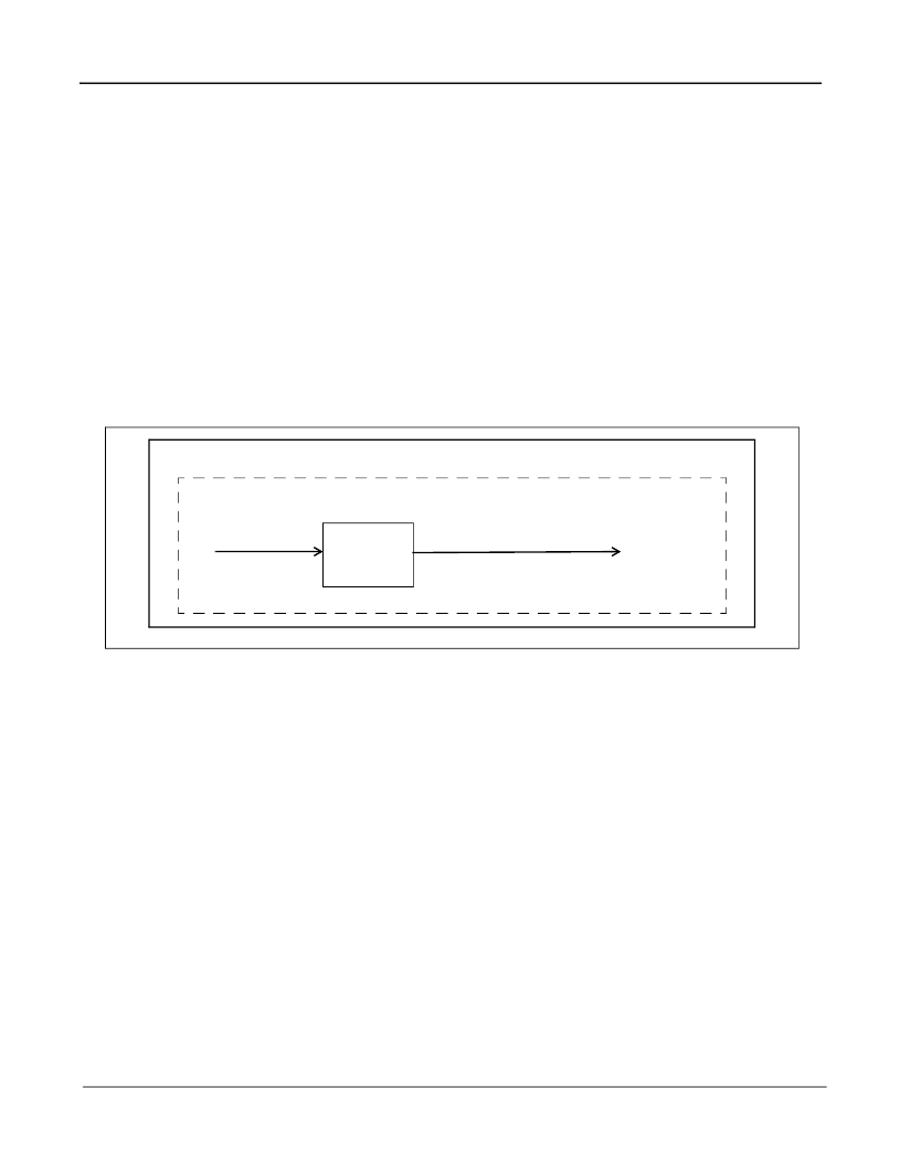
implementation of the synchronous clock generation is shown in Figure 35.
Figure 35 - Synchronous Source Multiplied to TDM Bus Rate by Internal PLL
The clock output from the PLL (PLLCLK for each of the DS1/E1 ports) is transmitted to the port’s corresponding
SToCLK multiplexer.
Synchronous Clock #2 (External PLL)
As an alternative to the internal PLL, an external PLL may be used to provide a synchronous clock for transmission
onto the TDM output bus. Using this method, a PRS-traceable signal from an external PLL is input to the MT90520
via the TDM_CLK pin. Since this is a “common” clock signal (i.e., one per device), TDM_CLK is routed to a
multiplexer, as shown previously in Figure 34. The output of this multiplexer is a common clock which is routed to
the clock selection multiplexers (one per port) in the “Interface to TDM sub-module”, detailed previously in
Section 4.7.2.1. The implementation of the synchronous clock generation is shown in Figure 36.
Clock Management Module
Digital
PLL
PLLCLK
8_kHz
MT90520
(generated by Network
Clock Divider Circuit
)
(Synchronous Clock #1)
To “Interface to
TDM Sub-Module”
Multiplexers &
“Synchronous
Clocking Circuit”
Multiplexers
相關(guān)PDF資料 |
PDF描述 |
|---|---|
| MT90520AG | 8-Port Primary Rate Circuit Emulation AAL1 SAR |
| MT9072 | Ultraframer DS3/E3/DS2/E2/DS1/E1/DS0 |
| MT9072AB | Ultraframer DS3/E3/DS2/E2/DS1/E1/DS0 |
| MT9072AV | Ultraframer DS3/E3/DS2/E2/DS1/E1/DS0 |
| MT90820 | Large Digital Switch |
相關(guān)代理商/技術(shù)參數(shù) |
參數(shù)描述 |
|---|---|
| MT90520AG | 制造商:Microsemi Corporation 功能描述:ATM SAR 2.048MBPS 2.5V CBR 456BGA - Trays |
| MT90520AG2 | 制造商:Microsemi Corporation 功能描述:ATM SAR 2.048MBPS 2.5V CBR 456BGA - Trays 制造商:Zarlink Semiconductor Inc 功能描述:ATM SAR 2.048MBPS 2.5V CBR 456BGA - Trays |
| MT90528 | 制造商:ZARLINK 制造商全稱:Zarlink Semiconductor Inc 功能描述:28-Port Primary Rate Circuit Emulation AAL1 SAR |
| MT90528AG | 制造商:ZARLINK 制造商全稱:Zarlink Semiconductor Inc 功能描述:28-Port Primary Rate Circuit Emulation AAL1 SAR |
| MT90528AG2 | 制造商:ZARLINK 制造商全稱:Zarlink Semiconductor Inc 功能描述:28-Port Primary Rate Circuit Emulation AAL1 SAR |
發(fā)布緊急采購(gòu),3分鐘左右您將得到回復(fù)。