- 您現(xiàn)在的位置:買賣IC網(wǎng) > PDF目錄98007 > M37902FCCHP 16-BIT, FLASH, 26 MHz, MICROCONTROLLER, PQFP100 PDF資料下載
參數(shù)資料
| 型號: | M37902FCCHP |
| 元件分類: | 微控制器/微處理器 |
| 英文描述: | 16-BIT, FLASH, 26 MHz, MICROCONTROLLER, PQFP100 |
| 封裝: | 14 X 14 MM, 0.50 MM PITCH, PLASTIC, LQFP-100 |
| 文件頁數(shù): | 72/143頁 |
| 文件大小: | 1148K |
| 代理商: | M37902FCCHP |
第1頁第2頁第3頁第4頁第5頁第6頁第7頁第8頁第9頁第10頁第11頁第12頁第13頁第14頁第15頁第16頁第17頁第18頁第19頁第20頁第21頁第22頁第23頁第24頁第25頁第26頁第27頁第28頁第29頁第30頁第31頁第32頁第33頁第34頁第35頁第36頁第37頁第38頁第39頁第40頁第41頁第42頁第43頁第44頁第45頁第46頁第47頁第48頁第49頁第50頁第51頁第52頁第53頁第54頁第55頁第56頁第57頁第58頁第59頁第60頁第61頁第62頁第63頁第64頁第65頁第66頁第67頁第68頁第69頁第70頁第71頁當(dāng)前第72頁第73頁第74頁第75頁第76頁第77頁第78頁第79頁第80頁第81頁第82頁第83頁第84頁第85頁第86頁第87頁第88頁第89頁第90頁第91頁第92頁第93頁第94頁第95頁第96頁第97頁第98頁第99頁第100頁第101頁第102頁第103頁第104頁第105頁第106頁第107頁第108頁第109頁第110頁第111頁第112頁第113頁第114頁第115頁第116頁第117頁第118頁第119頁第120頁第121頁第122頁第123頁第124頁第125頁第126頁第127頁第128頁第129頁第130頁第131頁第132頁第133頁第134頁第135頁第136頁第137頁第138頁第139頁第140頁第141頁第142頁第143頁
M37902FCCHP, M37902FGCHP, M37902FJCHP
SINGLE-CHIP 16-BIT CMOS MICROCOMPUTER
MITSUBISHI MICROCOMPUTERS
34
Notes 1: For details of the processor mode setting, see Table 3.
2: Processor mode bits = bits 0 and 1 of the processor mode register 0 (address 5E16).
3: The middle-order/high-order address output pins in the memory expansion or microprocessor mode can be switched to I/O port pins by the address/port
switch select bits of the port function control register (bits 2 to 0 at address 9216).
4: When the external data bus width for the chip select area, CS2, has been set to 8 bits, only in the access to area CS2, by the multiplexed bus select bit
of the CS2 control register H (bit 5 at address 8516), a multiplexed bus which performs the following operations with the time-sharing method is realized:
Output of address LA0 to LA7
Input/Output of data D0 to D7
5: When one of areas CS1/CS2/CS3 is accessed under the following conditions, pins D8 to D15 enter the floating state, and pin BHW outputs “H” level.
(They do not become I/O port pins.)
Pin BYTE is at Vss level.
One of bit 2s at addresses 8216, 8416, 8616 (the external data bus width select bit of the CS1/CS2/CS3 control register L) is set to “1” (external data bus
width = 8 bits).
6: In the memory expansion mode, by the corresponding select bits of the processor mode register 0 and 1 (addresses 5E16, 5F16), port pins P30, P40 to
P43 can operate as pins for RDY input, ALE output,
φ1 output, HLDA output, HOLD input, respectively.
In the microprocessor mode, by the above select bits, the above pins (RDY, ALE,
φ1, HLDA, HOLD) can operate as port pins P30, P40 to P43, respec-
tively.
In the single-chip mode, port pin P41 can operate as the
φ1 output pin by the above select bits.
7: In the memory expansion mode, port pin P44 can operate as the CS0 output pin by the CS0 output select bit of the CS0 control register L (bit 7 at address
8016).
8: In the memory expansion and microprocessor modes, port pins P45 to P47 can operate as the CS1/CS2/CS3 output pins by the CSi output select bits (i =
1 to 3) (bit 7s at addresses 8216, 8416, 8616).
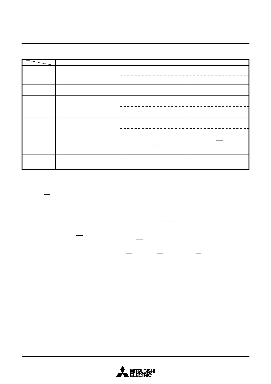
Table 6. Relationship between processor modes, memory area, and port function (2)
Single-chip mode
I/O port pin P40
I/O port pin P41
Clock
φ1 is output (Note 6).
I/O port pin P42
I/O port pin P43
I/O port pin P44
I/O port pins P45 to P47
Port pin P40
Port pin P41
Port pin P42
Port pin P43
Port pin P44
Port pins P45 to P47
Memory expansion mode
I/O port pin P40
Address latch enable signal
ALE is output (Note 6).
I/O port pin P41
Clock
φ1 is output (Note 6).
I/O port pin P42
Hold acknowledge signal
HLDA is output (Note 6).
I/O port pin P43
Hold request signal
HOLD is input (Note 6).
I/O port pin P44
Chip select signal CS0 is output
(Note 7).
I/O port pins P45 to P47
Chip select signals CS1 to CS3 are
output (Note 8).
Microprocessor mode
Address latch enable signal
ALE is output.
I/O port pin P40 (Note 6)
Clock
φ1 is output.
I/O port pin P41 (Note 6)
Hold acknowledge signal
HLDA is output.
I/O port pin P42 (Note 6)
Hold request signal
Signal HOLD is input.
I/O port pin P43 (Note 6)
Chip select signal CS0 is output.
I/O port pin P45 to P47
Chip select signals CS1 to CS3 are
output (Note 8).
相關(guān)PDF資料 |
PDF描述 |
|---|---|
| M37902FGCHP | 16-BIT, FLASH, 26 MHz, MICROCONTROLLER, PQFP100 |
| M37906F8CSP | 16-BIT, FLASH, 20 MHz, MICROCONTROLLER, PDIP42 |
| M37906F8CFP | 16-BIT, FLASH, 20 MHz, MICROCONTROLLER, PDSO42 |
| M37906F8CSP | 16-BIT, FLASH, 20 MHz, MICROCONTROLLER, PDIP42 |
| M37920S4CGP | 16-BIT, 20 MHz, MICROCONTROLLER, PQFP100 |
相關(guān)代理商/技術(shù)參數(shù) |
參數(shù)描述 |
|---|---|
| M37902FGCGP | 制造商:MITSUBISHI 制造商全稱:Mitsubishi Electric Semiconductor 功能描述:SINGLE-CHIP 16-BIT CMOS MICROCOMPUTER |
| M37902FGCHP | 制造商:MITSUBISHI 制造商全稱:Mitsubishi Electric Semiconductor 功能描述:SINGLE-CHIP 16-BIT CMOS MICROCOMPUTER |
| M37902FJCHP | 制造商:MITSUBISHI 制造商全稱:Mitsubishi Electric Semiconductor 功能描述:SINGLE-CHIP 16-BIT CMOS MICROCOMPUTER |
| M37903S4CHP | 制造商:RENESAS 制造商全稱:Renesas Technology Corp 功能描述:16-BIT CMOS MICROCOMPUTER |
| M37905F8CFP | 制造商:MITSUBISHI 制造商全稱:Mitsubishi Electric Semiconductor 功能描述:16-BIT CMOS MICROCOMPUTER |
發(fā)布緊急采購,3分鐘左右您將得到回復(fù)。