- 您現(xiàn)在的位置:買賣IC網(wǎng) > PDF目錄374310 > KAB01D100M (SAMSUNG SEMICONDUCTOR CO. LTD.) Tantalum Conformal-Coated Capacitor; Capacitance: 22uF; Voltage: 10V; Packaging: Tape & Reel PDF資料下載
參數(shù)資料
| 型號(hào): | KAB01D100M |
| 廠商: | SAMSUNG SEMICONDUCTOR CO. LTD. |
| 英文描述: | Tantalum Conformal-Coated Capacitor; Capacitance: 22uF; Voltage: 10V; Packaging: Tape & Reel |
| 中文描述: | 多芯片封裝存儲(chǔ)器 |
| 文件頁數(shù): | 19/72頁 |
| 文件大?。?/td> | 1378K |
| 代理商: | KAB01D100M |
第1頁第2頁第3頁第4頁第5頁第6頁第7頁第8頁第9頁第10頁第11頁第12頁第13頁第14頁第15頁第16頁第17頁第18頁當(dāng)前第19頁第20頁第21頁第22頁第23頁第24頁第25頁第26頁第27頁第28頁第29頁第30頁第31頁第32頁第33頁第34頁第35頁第36頁第37頁第38頁第39頁第40頁第41頁第42頁第43頁第44頁第45頁第46頁第47頁第48頁第49頁第50頁第51頁第52頁第53頁第54頁第55頁第56頁第57頁第58頁第59頁第60頁第61頁第62頁第63頁第64頁第65頁第66頁第67頁第68頁第69頁第70頁第71頁第72頁
KAB0xD100M - TxGP
Revision 1.11
August 2003
- 19 -
MCP MEMORY
SEC Only
Unlock Bypass
The NOR Flash memory provides the unlock bypass mode to save its program time. The mode is invoked by the unlock bypass com-
mand sequence. Unlike the standard program command sequence that contains four bus cycles, the unlock bypass program com-
mand sequence comprises only two bus cycles.
The unlock bypass mode is engaged by issuing the unlock bypass command sequence which is comprised of three bus cycles. Writ-
ing first two unlock cycles is followed by a third cycle containing the unlock bypass command (20H). Once the device is in the unlock
bypass mode, the unlock bypass program command sequence is necessary to program in this mode. The unlock bypass program
command sequence is comprised of only two bus cycles; writing the unlock bypass program command
(A0H) is followed by the pro-
gram address and data. This command sequence is the only valid one for programming the device in the unlock bypass mode.
The unlock bypass reset command sequence is the only valid command sequence to exit the unlock bypass mode. The unlock
bypass reset command sequence consists of two bus cycles. The first cycle must contain the data (90H). The second cycle contains
only the data (00H). Then, the device returns to the read mode.
Chip Erase
To erase a chip is to write 1
′
s into the entire memory array by executing the Internal Erase Routine. The Chip Erase requires six bus
cycles to write the command sequence. The erase set-up command is written after first two "unlock" cycles. Then, there are two
more write cycles prior to writing the chip erase command. The Internal Erase Routine automatically pre-programs and verifies the
entire memory for an all zero data pattern prior to erasing. The automatic erase begins on the rising edge of the last WE or CE
R
pulse in the command sequence and terminates when DQ7 is "1". After that the device returns to the read mode.
Block Erase
To erase a block is to write 1
′
s into the desired memory block by executing the Internal Erase Routine. The Block Erase requires six
bus cycles to write the command sequence shown in Table 5. After the first two "unlock" cycles, the erase setup command (80H) is
written at the third cycle. Then there are two more "unlock" cycles followed by the Block Erase command. The Internal Erase Routine
automatically pre-programs and verifies the entire memory prior to erasing it. The block address is latched on the falling edge of WE
or CE
R
, while the Block Erase command is latched on the rising edge of WE or CE
R
.
Multiple blocks can be erased sequentially by writing the six bus-cycle operation in Fig 7. Upon completion of the last cycle for the
Block Erase, additional block address and the Block Erase command (30H) can be written to perform the Multi-Block Erase. An 50us
(typical) "time window" is required between the Block Erase command writes. The Block Erase command must be written within the
50us "time window", otherwise the Block Erase command will be ignored. The 50us "time window" is reset when the falling edge of
the WE occurs within the 50us of "time window" to latch the Block Erase command. During the 50us of "time window", any command
other than the Block Erase or the Erase Suspend command written to the device will reset the device to read mode. After the 50 us
of "time window", the Block Erase command will initiate the Internal Erase Routine to erase the selected blocks. Any Block Erase
address and command following the exceeded "time window" may or may not be accepted. No other commands will be recognized
except the Erase Suspend command.
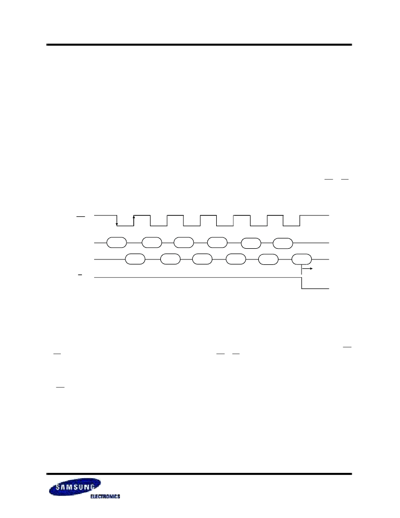
Figure 6. Chip Erase Command Sequence
WE
555H/
AAAH
2AAH/
555H
555H/
AAAH
AAH
55H
80H
555H
AAAH
Chip Erase
Start
DQ15-DQ0
2AAH/
555H
AAH
55H
10H
R/B
R
555H/
AAAH
A21
~
A0(x16)/
A21
~
A-1(x8)
相關(guān)PDF資料 |
PDF描述 |
|---|---|
| KAB02D100M-TLGP | Tantalum Conformal-Coated Capacitor; Capacitance: 22uF; Voltage: 10V; Packaging: Tape & Reel |
| KAB01D100M-TNGP | CONNECTOR ACCESSORY |
| KAB02D100M-TNGP | CONNECTOR ACCESSORY |
| KAB3403DN | White LED Step-Up Converter |
| KAB3403T | White LED Step-Up Converter |
相關(guān)代理商/技術(shù)參數(shù) |
參數(shù)描述 |
|---|---|
| KAB01D100M-TLGP | 制造商:SAMSUNG 制造商全稱:Samsung semiconductor 功能描述:Multi-Chip Package MEMORY |
| KAB01D100M-TNGP | 制造商:SAMSUNG 制造商全稱:Samsung semiconductor 功能描述:Multi-Chip Package MEMORY |
| KAB02D100M-TLGP | 制造商:SAMSUNG 制造商全稱:Samsung semiconductor 功能描述:Multi-Chip Package MEMORY |
| KAB02D100M-TNGP | 制造商:SAMSUNG 制造商全稱:Samsung semiconductor 功能描述:Multi-Chip Package MEMORY |
| KAB03D100M-TLGP | 制造商:SAMSUNG 制造商全稱:Samsung semiconductor 功能描述:Multi-Chip Package MEMORY |
發(fā)布緊急采購,3分鐘左右您將得到回復(fù)。