- 您現(xiàn)在的位置:買賣IC網(wǎng) > PDF目錄370782 > HYB18T512160AF-3.7 (INFINEON TECHNOLOGIES AG) 512-Mbit DDR2 SDRAM PDF資料下載
參數(shù)資料
| 型號: | HYB18T512160AF-3.7 |
| 廠商: | INFINEON TECHNOLOGIES AG |
| 英文描述: | 512-Mbit DDR2 SDRAM |
| 中文描述: | 512兆位DDR2 SDRAM的 |
| 文件頁數(shù): | 91/117頁 |
| 文件大小: | 2102K |
| 代理商: | HYB18T512160AF-3.7 |
第1頁第2頁第3頁第4頁第5頁第6頁第7頁第8頁第9頁第10頁第11頁第12頁第13頁第14頁第15頁第16頁第17頁第18頁第19頁第20頁第21頁第22頁第23頁第24頁第25頁第26頁第27頁第28頁第29頁第30頁第31頁第32頁第33頁第34頁第35頁第36頁第37頁第38頁第39頁第40頁第41頁第42頁第43頁第44頁第45頁第46頁第47頁第48頁第49頁第50頁第51頁第52頁第53頁第54頁第55頁第56頁第57頁第58頁第59頁第60頁第61頁第62頁第63頁第64頁第65頁第66頁第67頁第68頁第69頁第70頁第71頁第72頁第73頁第74頁第75頁第76頁第77頁第78頁第79頁第80頁第81頁第82頁第83頁第84頁第85頁第86頁第87頁第88頁第89頁第90頁當前第91頁第92頁第93頁第94頁第95頁第96頁第97頁第98頁第99頁第100頁第101頁第102頁第103頁第104頁第105頁第106頁第107頁第108頁第109頁第110頁第111頁第112頁第113頁第114頁第115頁第116頁第117頁
Data Sheet
91
Rev. 1.3, 2005-01
09112003-SDM9-IQ3P
HYB18T512[40/80/16]0AF–[3/3S/3.7/5]
512-Mbit DDR2 SDRAM
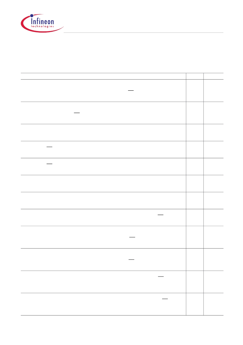
Currents Measurement Specifications and Conditions
6
Currents Measurement Specifications and Conditions
Table 44
Parameter
Operating Current -
One bank Active - Precharge
t
CK
=
t
CK(IDD)
,
t
RC
=
t
RC(IDD)
,
t
RAS
=
t
RAS.MIN(IDD)
, CKE is HIGH, CS is HIGH between valid
commands. Address and control inputs are switching; Databus inputs are switching.
Operating Current - One bank Active - Read - Precharge
I
OUT
= 0 mA, BL = 4,
t
CK
=
t
CK(IDD)
,
t
RC
=
t
RC(IDD)
,
t
RAS
=
t
RAS.MIN(IDD)
,
t
RCD
=
t
RCD(IDD)
, AL = 0,
CL = CL(IDD); CKE is HIGH, CS is HIGH between valid commands. Address and control
inputs are switching; Databus inputs are switching.
Precharge Power-Down Current
All banks idle; CKE is LOW;
t
CK
=
t
CK(IDD)
;Other control and address inputs are stable; Data
bus inputs are floating
.
Precharge Standby Current
All banks idle; CS is HIGH; CKE is HIGH;
t
CK
=
t
CK(IDD)
; Other control and address inputs are
switching, Data bus inputs are switching
.
Precharge Quiet Standby Current
All banks idle; CS is HIGH; CKE is HIGH;
t
CK
=
t
CK(IDD)
; Other control and address inputs are
stable, Data bus inputs are floating.
Active Power-Down Current
All banks open;
t
CK
=
t
CK(IDD)
, CKE is LOW; Other control and address inputs are stable; Data
bus inputs are floating. MRS A12 bit is set to “0” (Fast Power-down Exit).
Active Power-Down Current
All banks open;
t
CK
=
t
CK(IDD)
, CKE is LOW; Other control and address inputs are stable, Data
bus inputs are floating. MRS A12 bit is set to 1 (Slow Power-down Exit);
Active Standby Current
All banks open;
t
CK
=
t
CK(IDD)
;
t
RAS
=
t
RAS.MAX(IDD)
,
t
RP
=
t
RP(IDD)
; CKE is HIGH, CS is HIGH
between valid commands. Address inputs are switching; Data Bus inputs are switching;
Operating Current
Burst Read: All banks open; Continuous burst reads; BL = 4; AL = 0, CL = CL
(IDD)
;
t
CK
=
t
CK(IDD)
;
t
RAS
=
t
RAS.MAX.(IDD)
,
t
RP
=
t
RP(IDD)
; CKE is HIGH, CS is HIGH between valid
commands. Address inputs are switching; Data Bus inputs are switching;
I
OUT
= 0 mA.
Operating Current
Burst Write: All banks open; Continuous burst writes; BL = 4; AL = 0, CL = CL
(IDD)
;
t
CK
=
t
CK(IDD)
;
t
RAS
=
t
RAS.MAX(IDD)
,
t
RP
=
t
RP(IDD)
; CKE is HIGH, CS is HIGH between valid
commands. Address inputs are switching; Data Bus inputs are switching;
Burst Refresh Current
t
CK
=
t
CK(IDD)
, Refresh command every
t
RFC
=
t
RFC(IDD)
interval, CKE is HIGH, CS is HIGH
between valid commands, Other control and address inputs are switching, Data bus inputs
are switching.
Distributed Refresh Current
t
CK
=
t
CK(IDD)
, Refresh command every
t
REFI
= 7.8
μ
s interval, CKE is LOW and CS is HIGH
between valid commands, Other control and address inputs are switching, Data bus inputs
are switching.
I
DD
Measurement Conditions
Symbol Note
I
DD0
1)2)3)4)5)6)
I
DD1
1)2)3)4)5)6)
I
DD2P
1)2)3)4)5)6)
I
DD2N
1)2)3)4)5)6)
I
DD2Q
1)2)3)4)5)6)
I
DD3P(0)
1)2)3)4)5)6)
I
DD3P(1)
1)2)3)4)5)6)
I
DD3N
1)2)3)4)5)6)
I
DD4R
1)2)3)4)5)6)
I
DD4W
1)2)3)4)5)6)
I
DD5B
1)2)3)4)5)6)
I
DD5D
1)2)3)4)5)6)
相關(guān)PDF資料 |
PDF描述 |
|---|---|
| HYB18T512160AF-3S | 512-Mbit DDR2 SDRAM |
| HYB18T512400AF-3 | 512-Mbit DDR2 SDRAM |
| HYB18T512400AF-3S | 512-Mbit DDR2 SDRAM |
| HYB18T512800AF-3 | 512-Mbit DDR2 SDRAM |
| HYB18T512800AF-3.7 | 512-Mbit DDR2 SDRAM |
相關(guān)代理商/技術(shù)參數(shù) |
參數(shù)描述 |
|---|---|
| HYB18T512161BF-25 | 制造商:Qimonda 功能描述:SDRAM, DDR, 32M x 16, 84 Pin, Plastic, BGA |
| HYB18T512400AF-5 | 制造商:Intersil Corporation 功能描述:SDRAM, DDR, 128M x 4, 60 Pin, Plastic, BGA |
| HYB18T512400BF-3S | 制造商:Qimonda 功能描述: |
| HYB18T512800AF-3S | 制造商:Qimonda 功能描述: 制造商:Infineon Technologies AG 功能描述:32M X 16 DDR DRAM, 0.45 ns, PBGA84 |
| HYB18T512800BF-2.5 | 功能描述:IC DDR2 SDRAM 512MBIT 60TFBGA RoHS:是 類別:集成電路 (IC) >> 存儲器 系列:- 標準包裝:60 系列:- 格式 - 存儲器:EEPROMs - 串行 存儲器類型:EEPROM 存儲容量:16K (2K x 8) 速度:2MHz 接口:SPI 3 線串行 電源電壓:2.5 V ~ 5.5 V 工作溫度:-40°C ~ 85°C 封裝/外殼:8-DIP(0.300",7.62mm) 供應商設(shè)備封裝:8-PDIP 包裝:管件 產(chǎn)品目錄頁面:1449 (CN2011-ZH PDF) |
發(fā)布緊急采購,3分鐘左右您將得到回復。