- 您現(xiàn)在的位置:買賣IC網(wǎng) > PDF目錄1996 > HMC700LP4E (Hittite Microwave Corporation)IC FRACT-N PLL 16BIT 24QFN PDF資料下載
參數(shù)資料
| 型號: | HMC700LP4E |
| 廠商: | Hittite Microwave Corporation |
| 文件頁數(shù): | 10/26頁 |
| 文件大?。?/td> | 0K |
| 描述: | IC FRACT-N PLL 16BIT 24QFN |
| 標(biāo)準(zhǔn)包裝: | 1 |
| 類型: | 整數(shù) N/小數(shù) N 分頻 |
| PLL: | 是 |
| 輸入: | CMOS |
| 輸出: | CMOS |
| 電路數(shù): | 1 |
| 比率 - 輸入:輸出: | 1:1 |
| 差分 - 輸入:輸出: | 是/無 |
| 頻率 - 最大: | 8GHz |
| 除法器/乘法器: | 是/無 |
| 電源電壓: | 3.3V,5V |
| 工作溫度: | -40°C ~ 85°C |
| 安裝類型: | 表面貼裝 |
| 封裝/外殼: | 24-VQFN 裸露焊盤 |
| 供應(yīng)商設(shè)備封裝: | 24-QFN 裸露焊盤(4x4) |
| 包裝: | 標(biāo)準(zhǔn)包裝 |
| 其它名稱: | 1127-1064-6 |
第1頁第2頁第3頁第4頁第5頁第6頁第7頁第8頁第9頁當(dāng)前第10頁第11頁第12頁第13頁第14頁第15頁第16頁第17頁第18頁第19頁第20頁第21頁第22頁第23頁第24頁第25頁第26頁

For price, delivery and to place orders: Hittite Microwave Corporation, 2 Elizabeth Drive, Chelmsford, MA 01824
978-250-3343 tel 978-250-3373 fax Order On-line at www.hittite.com
Application Support: apps@hittite.com
P
LL
-
F
r
a
c
t
io
n
a
L-
n
-
S
M
t
0
0 - 18
HMC700LP4 / 700LP4E
v11.0411
8 GHz 16-Bit Fractional-N PLL
General Purpose Output (GPO) Pins
the HMc700LP4(E) also supports a simple two pin GPo bus implemented on pins D1 and D0. GPo operation
requires that GPo output pads be enabled via gpio_pads_en (table 15). two bit arbitrary data may be written to the
GPo outputs via register gpo_test, when gpo_select is first set to 10d (table 20). other test waveforms, described
in table 20, may be output to the GPo pins according to the value written to gpo_select. if the GPo outputs are not
used, and it is desirable that they are as quiet as possible then the GPo pads should be disabled via gpio_pads_en
(table 15) and gpo_select set to a value that has a static source, such as 10d.
Register Map
Note: For read operations from register 00h, it is read only containing the chip iD. current Hittite synthesizer chip
iDs are shown in table 6.
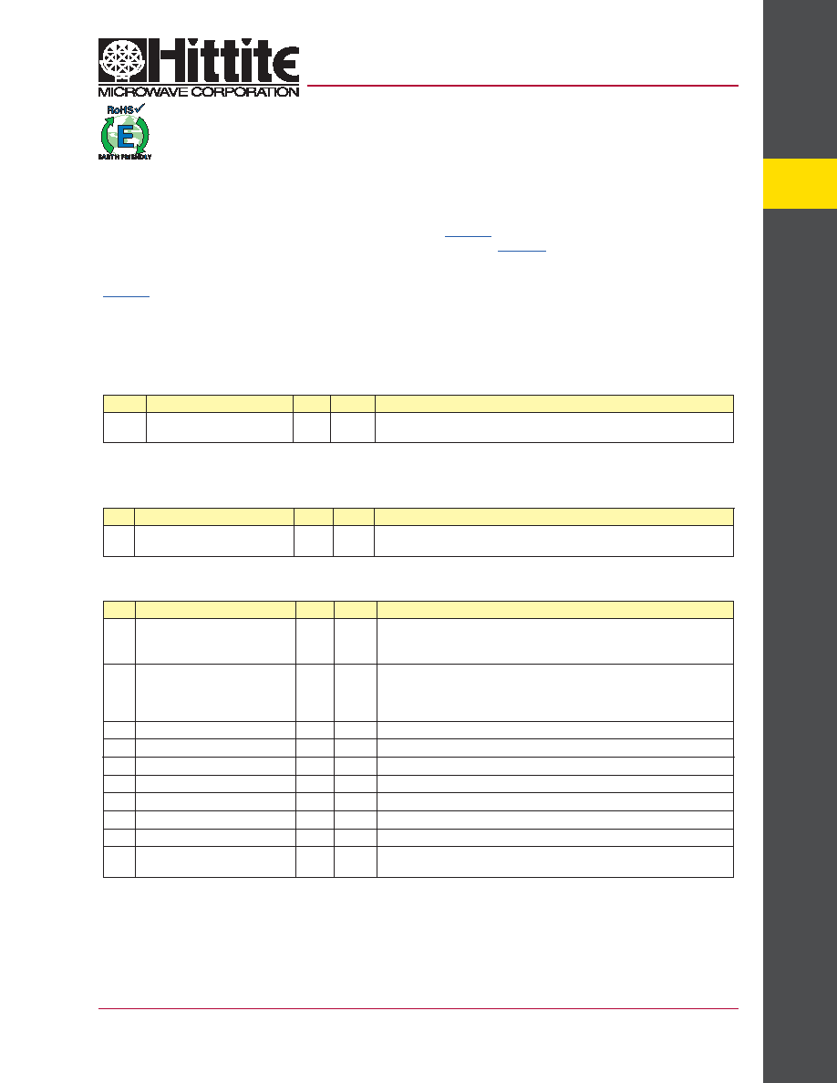
Table 6. Reg00h ID (Read Only) Register
Bit
name
Width
Default
Description
[23:0]
chip_iD
24
478708h
or 485901
Part number, Description HMc700LP4, 16-Bit 5.5V
For write operations to register 00h, it is a Write only strobe register as defined in table 7.
Table 7. Reg00h RST Strobe Register
Bit
name
Width
Default
Description
[0]
rst_swrst
1
n/a
Strobe (WritE onLY) generates soft reset. resets all digital and registers to
default states.
Table 8. Reg 01h RST Register
Bit
name
Width
Default
Description
[0]
rst_chipen_pin_select
1
1 = chip enable via cE pin, cE (Pin 23) enables chip. cE low puts chip in power
down.
0 = chip enable via SPi (rst_chipen_from_spi), cE Pin is ignored
[1]
rst_chipen_from_spi
1
0
1= chip Enable when rst_chipen_pin_select = 0
0= Power Down when rst_chipen_pin_select = 0
see Power Down Mode description and csp_enable reg07 <20>
if rst_chipen_pin_select =1 this register is ignored
[2]
rst_chipen_digclks_keep_on
1
0
keeps digital clocks on when chip is Power Down from any source
[3]
rst_chipen_bias_keep_on
1
0
keeps chip internal bias generators on when chip is Power Down from any source
[4]
rst_chipen_pfd_keep_on
1
0
keeps internal PFD block on when chip is Power Down from any source
[5]
rst_chipen_chp_keep_on
1
0
keeps internal charge Pump block on when chip is Power Down from any source
[6]
rst_chipen_refbuf_keep_on
1
0
keeps reference path buffer on when chip is Power Down from any source
[7]
rst_chipen_vcobuf_keep_on
1
0
keeps Vco path rF buffer on when chip is Power Down from any source
[8]
rst_chipen_dig_io_keep_on
1
0
keeps digital io pins on when chip is Power Down from any source
[9]
rst_chipen_rdiv_fe_sync
1
0
tri-states the PFD on the next falling edge of the ref clock and also puts the chip
to sleep
相關(guān)PDF資料 |
PDF描述 |
|---|---|
| HMC703LP4E | IC FRACT-N PLL W/SWEEPR 24QFN |
| HMC704LP4E | IC FRACT-N PLL 16BIT 24QFN |
| HMC830LP6GE | IC FRACT-N PLL W/VCO 40QFN |
| HMP8117CNZ | IC VIDEO DECODER NTSC/PAL 80PQFP |
| HMP8156ACNZ | IC VIDEO ENCODER NTSC/PAL 64MQFP |
相關(guān)代理商/技術(shù)參數(shù) |
參數(shù)描述 |
|---|---|
| HMC700LP4ETR | 制造商:Hittite Microwave Corp 功能描述:IC FRACT-N PLL 16BIT 24QFN 制造商:Hittite Microwave Corp 功能描述:HMC700 Series 8 GHz 16-Bit Prescaler Fractional-N PLL - 4x4 mm QFN-24 |
| HMC701LP6C | 制造商:HITTITE 制造商全稱:Hittite Microwave Corporation 功能描述:8 GHz 16-BIT FRACTIONAL-N SYNTHESIZER |
| HMC701LP6C_10 | 制造商:HITTITE 制造商全稱:Hittite Microwave Corporation 功能描述:8 GHz 16-BIT FRACTIONAL-N SYNTHESIZER |
| HMC701LP6CE | 制造商:Hittite Microwave Corp 功能描述:IC SYNTHESIZER W/SWEEPER 40-QFN |
| HMC702LP6CE | 制造商:Hittite Microwave Corp 功能描述:IC SYNTHESIZER W/SWEEPER 40-QFN |
發(fā)布緊急采購,3分鐘左右您將得到回復(fù)。