- 您現(xiàn)在的位置:買(mǎi)賣(mài)IC網(wǎng) > PDF目錄383012 > GMS87C7216LQ (Electronic Theatre Controls, Inc.) 8-BIT SINGLE-CHIP MICROCONTROLLERS PDF資料下載
參數(shù)資料
| 型號(hào): | GMS87C7216LQ |
| 廠(chǎng)商: | Electronic Theatre Controls, Inc. |
| 元件分類(lèi): | 數(shù)學(xué)處理器 |
| 英文描述: | 8-BIT SINGLE-CHIP MICROCONTROLLERS |
| 中文描述: | 8位單晶片微控制器 |
| 文件頁(yè)數(shù): | 35/121頁(yè) |
| 文件大小: | 1645K |
| 代理商: | GMS87C7216LQ |
第1頁(yè)第2頁(yè)第3頁(yè)第4頁(yè)第5頁(yè)第6頁(yè)第7頁(yè)第8頁(yè)第9頁(yè)第10頁(yè)第11頁(yè)第12頁(yè)第13頁(yè)第14頁(yè)第15頁(yè)第16頁(yè)第17頁(yè)第18頁(yè)第19頁(yè)第20頁(yè)第21頁(yè)第22頁(yè)第23頁(yè)第24頁(yè)第25頁(yè)第26頁(yè)第27頁(yè)第28頁(yè)第29頁(yè)第30頁(yè)第31頁(yè)第32頁(yè)第33頁(yè)第34頁(yè)當(dāng)前第35頁(yè)第36頁(yè)第37頁(yè)第38頁(yè)第39頁(yè)第40頁(yè)第41頁(yè)第42頁(yè)第43頁(yè)第44頁(yè)第45頁(yè)第46頁(yè)第47頁(yè)第48頁(yè)第49頁(yè)第50頁(yè)第51頁(yè)第52頁(yè)第53頁(yè)第54頁(yè)第55頁(yè)第56頁(yè)第57頁(yè)第58頁(yè)第59頁(yè)第60頁(yè)第61頁(yè)第62頁(yè)第63頁(yè)第64頁(yè)第65頁(yè)第66頁(yè)第67頁(yè)第68頁(yè)第69頁(yè)第70頁(yè)第71頁(yè)第72頁(yè)第73頁(yè)第74頁(yè)第75頁(yè)第76頁(yè)第77頁(yè)第78頁(yè)第79頁(yè)第80頁(yè)第81頁(yè)第82頁(yè)第83頁(yè)第84頁(yè)第85頁(yè)第86頁(yè)第87頁(yè)第88頁(yè)第89頁(yè)第90頁(yè)第91頁(yè)第92頁(yè)第93頁(yè)第94頁(yè)第95頁(yè)第96頁(yè)第97頁(yè)第98頁(yè)第99頁(yè)第100頁(yè)第101頁(yè)第102頁(yè)第103頁(yè)第104頁(yè)第105頁(yè)第106頁(yè)第107頁(yè)第108頁(yè)第109頁(yè)第110頁(yè)第111頁(yè)第112頁(yè)第113頁(yè)第114頁(yè)第115頁(yè)第116頁(yè)第117頁(yè)第118頁(yè)第119頁(yè)第120頁(yè)第121頁(yè)
GMS81C7208/7216
FEB. 2005 Ver 1.04
31
9. I/O PORTS
The GMS81C7208/16 has six ports (R0, R2, R3, R4, R5 and R6),
and LCD segment port SEG0~SEG11 and SEG16~SEG20 and
LCD common port COM0~COM3, which are multiplexed with
SEG24~SEG26.
These ports pins may be multiplexed with an alternate function
for the peripheral features on the device. In general, in a initial re-
set state, R0,R2,R3 ports are used as a general purpose input port
and R4, R5 and R6 ports are used as LCD segment drive output
port.
9.1 Port Data Registers
Port Data Registers
The Port Data Registers in I/O buffer in each six ports
(R0,R2,R3,R4,R5,R6) are represented as a Type D flip-flop,
which will clock in a value from the internal bus in response to a
"write to data register" signal from the CPU. The Q output of the
flip-flop is placed on the internal bus in response to a "read data
register" signal from the CPU. The level of the port pin itself is
placed on the internal bus in response to "read data register" sig-
nal from the CPU. Some instructions that read a port activating
the "read register" signal, and others activating the "read pin" sig-
nal
Port Direction Registers
All pins have data direction registers which can define these ports
as output or input. A "1" in the port direction register configure
the corresponding port pin as output. Conversely, write "0" to the
corresponding bit to specify it as input pin. For example, to use
the even numbered bit of R0 as output ports and the odd num-
bered bits as input ports, write “55
H
” to address 0C8
H
(R0 port
direction register) during initial setting as shown in Figure 9-1.
Figure 9-1 Example of Port I/O Assignment
All the port direction registers in the MCU have 0 written to them
by reset function. On the other hand, its initial status is input.
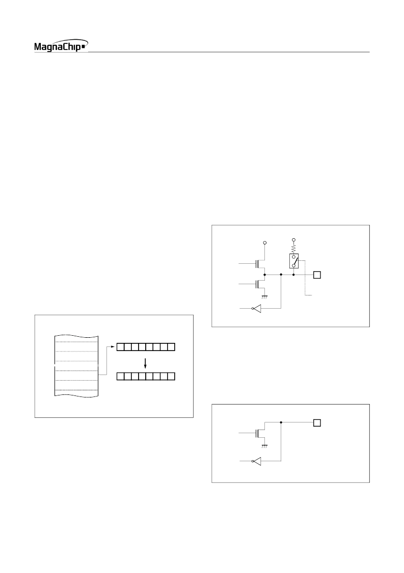
Pull-up Control Registers
The R0, R2 and R3 ports have internal pull-up resistors.
Figure 9-2 shows a functional diagram of a typical pull-up port.
It is connected or disconnected by pull-up control register
(PUR
n
). The value of that resistor is typically 160k
.
When a port is used as input, input logic is firmly either low or
high, therefore external pull-down or pull-up resisters are re-
quired practically. The GMS81C7208/16 has internal pull-up, it
can be logic high by pull-up that can be able to configure either
connect or disconnect individually by pull-up control registers
R0PU, R2PU and R3PU.
When ports are configured as inputs and pull-up resistor is select-
ed by software, they are pulled to high.
Figure 9-2 Pull-up Port Structure
Open Drain Port Registers
The R0, R2 and R3 ports have open drain port resistors
R0CR~R3CR.
Figure 9-3 shows a open drain port configuration by control reg-
ister. It is selected as either push-pull port or open-drain port by
R0CR, R1CR, R2CR and R3CR.
Figure 9-3 Open Drain Port Structure
I : INPUT PORT
O : OUTPUT PORT
WRITE “55
H
” TO PORT R0 DIRECTION REGISTER
0
7
1
6
0
5
1
4
0
3
1
2
0
1
1
0
I
O
I
O
I
O
I
O
R0 DATA
R0 DIRECTION
R1 DATA
R1 DIRECTION
0C0H
0C1H
0C8H
0C9H
BIT
7
6
5
4
3
2
1
0
PORT
~
~
PULL-UP RESISTOR
Typ. 160k
PORT PIN
1: Connect
0: Disconnect
Pull-up control bit
VDD
GND
VDD
PORT PIN
1: Open drain
0: Push-pull
Open drain port selection bit
GND
相關(guān)PDF資料 |
PDF描述 |
|---|---|
| GNR20D101K | VARISTOR |
| GNR20D102K | VARISTOR |
| GNR20D112K | VARISTOR |
| GNR20D121K | VARISTOR |
| GNR20D151K | VARISTOR |
相關(guān)代理商/技術(shù)參數(shù) |
參數(shù)描述 |
|---|---|
| GMS87C7216Q | 制造商:未知廠(chǎng)家 制造商全稱(chēng):未知廠(chǎng)家 功能描述:8-BIT SINGLE-CHIP MICROCONTROLLERS |
| GM-S-88 | 功能描述:以太網(wǎng)和電信連接器 8P8C R/A PCB SHIELD LOW PROFILE BLACK RoHS:否 制造商:Pulse 產(chǎn)品:Modular Jacks 性能類(lèi)別: USOC 代碼:RJ45 位置/觸點(diǎn)數(shù)量: 安裝風(fēng)格:Through Hole 端口數(shù)量:1 x 1 型式:Female 屏蔽: 電流額定值: 電壓額定值: 觸點(diǎn)電鍍: 外殼材料:Thermoplastic IP 等級(jí): |
| GM-S-88-50 | 功能描述:以太網(wǎng)和電信連接器 8P8C R/A PCB SHIELD LOW PROFILE BLK 50u RoHS:否 制造商:Pulse 產(chǎn)品:Modular Jacks 性能類(lèi)別: USOC 代碼:RJ45 位置/觸點(diǎn)數(shù)量: 安裝風(fēng)格:Through Hole 端口數(shù)量:1 x 1 型式:Female 屏蔽: 電流額定值: 電壓額定值: 觸點(diǎn)電鍍: 外殼材料:Thermoplastic IP 等級(jí): |
| GMS90 | 制造商:HYNIX 制造商全稱(chēng):Hynix Semiconductor 功能描述:8-BIT SINGLE-CHIP MICROCONTROLLERS |
| GMS90C31 | 制造商:HYNIX 制造商全稱(chēng):Hynix Semiconductor 功能描述:HYNIX SEMICONDUCTOR INC. 8-BIT SINGLE-CHIP MICROCONTROLLERS |
發(fā)布緊急采購(gòu),3分鐘左右您將得到回復(fù)。