- 您現(xiàn)在的位置:買賣IC網(wǎng) > PDF目錄369482 > BR1570 WarpLink Reference Design Platform PDF資料下載
參數(shù)資料
| 型號: | BR1570 |
| 英文描述: | WarpLink Reference Design Platform |
| 中文描述: | WarpLink參考設(shè)計平臺 |
| 文件頁數(shù): | 16/24頁 |
| 文件大小: | 492K |
| 代理商: | BR1570 |
WarpLink Reference Design Platform
16
For More Information On This Product,
Go to: www.freescale.com
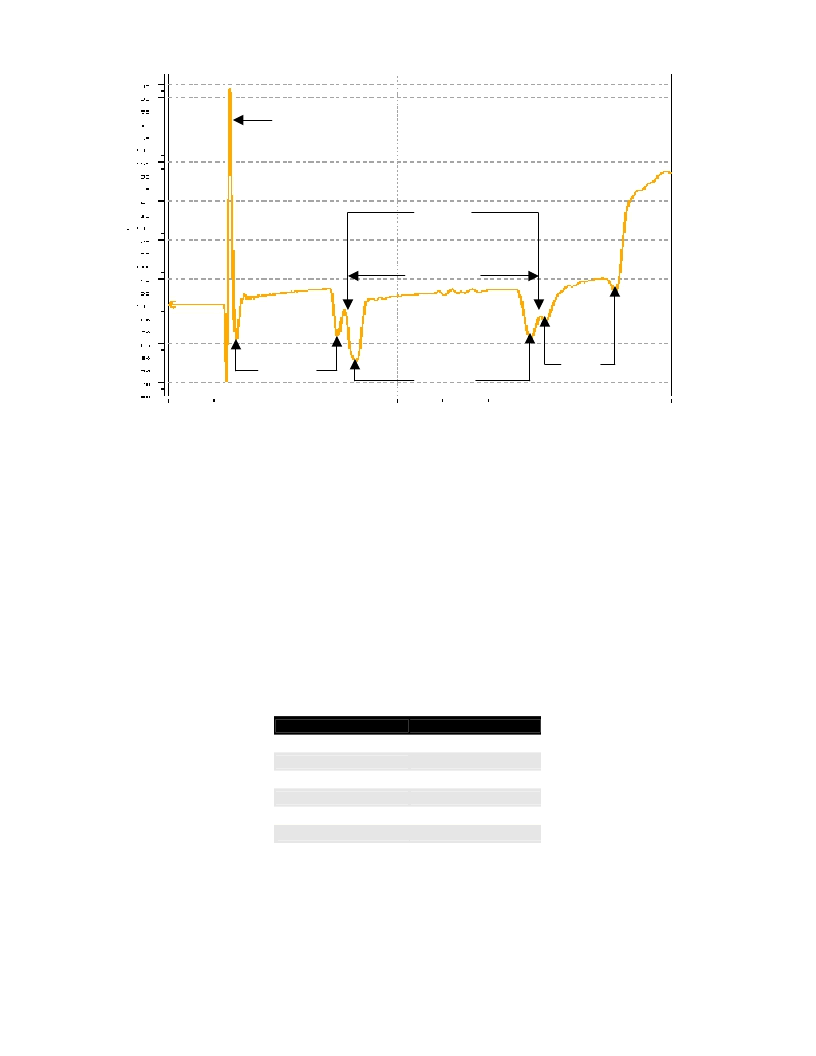
Figure 12. TDR of 10-inch Backplane with Through Vias
A comparison of the impedance profiles show that the
through
via produce smaller impedance discontinuity, Figure 12, than the stub via
case, Figure 11. The package model presents a significant discontinuity in the simulation of the WarpLink interconnect, for both via cases.
The large inductive spike is likely due to the lumped-element package model used in the simulations.
The discontinuity of the ERmet ZD connector reflected its ability to transmit 5Gbps signals. The peak impedance level within the
connector region was approximately 95-98 ohms. The effects of the vias on both the daughter card and backplane influence this level due
to risetime roll-off of the TDR pulse. The lossy characteristic of the transmission line is evident as seen in the increasing impedance along
the length of the TDR profile.
WARPLINK REFERENCE SYSTEM CLOCK SIMULATIONS
The clock architecture for the WarpLink Reference Design Platform is point-to-point. The clock operates at a digital frequency of 156.25
MHz. This data rate allowed the clock to be connected to the daughter card thought a standard 2 mm hard metric connector, the ERmet 2
mm-HM. The interconnect path models used for the clock simulations are almost identical to that of the gigabit WarpLink models. The
main differences were the replacement of the ERmet ZD with the ERmet 2 mm-HM connectors and the inclusion of the clock driver and
receivers in place of the WarpLink devices.
Table 6. Simulation Matrix Values
Variables
Clock Buffer Device
Temperature
Process
Supply voltage (3.3 V
±
10%)
Interconnect
Backplane trace length
Line card and switch card vias
Range
0
°
C, 25
°
C, and 100
°
C
SS, TT, FF
3.0 V, 3.3 V, and 3.6 V
2, 10, and 20 inches
One layer transition with stub
and full board transition
The variables and range of the simulation matrix for the clock are shown in Table 6. The results of the simulations, exemplified by the
waveform in Figure 13, show little distortion and a well-controlled clock signal.
Reference
WarpLink
Package
Daughter Card
T-Line
Daughter
Card Via
Ermet-ZD
Connector
Backplane T-Line
Backplane Via
Daughter Card
T-Line
Daughter
Card Via
Open Circuit
Termination
F
Freescale Semiconductor, Inc.
n
.
相關(guān)PDF資料 |
PDF描述 |
|---|---|
| BR200A | TRANSISTOR | BJT | NPN | 50V V(BR)CEO | 20A I(C) | TO-210AC |
| BR200B | TRANSISTOR | BJT | NPN | 50V V(BR)CEO | 20A I(C) | TO-210AC |
| BR201A | TRANSISTOR | BJT | NPN | 75V V(BR)CEO | 20A I(C) | TO-210AC |
| BR201B | TRANSISTOR | BJT | NPN | 75V V(BR)CEO | 20A I(C) | TO-210AC |
| BR211-140AMO | SINGLE BIDIRECTIONAL BREAKOVER DIODE|157V V(BO) MAX|1A I(S)|SOD-84 |
相關(guān)代理商/技術(shù)參數(shù) |
參數(shù)描述 |
|---|---|
| BR158 | 功能描述:橋式整流器 15A 800V RoHS:否 制造商:Vishay 產(chǎn)品:Single Phase Bridge 峰值反向電壓:1000 V 最大 RMS 反向電壓: 正向連續(xù)電流:4.5 A 最大浪涌電流:450 A 正向電壓下降:1 V 最大反向漏泄電流:10 uA 功率耗散: 最大工作溫度:+ 150 C 長度:30.3 mm 寬度:4.1 mm 高度:20.3 mm 安裝風(fēng)格:Through Hole 封裝 / 箱體:SIP-4 封裝:Tube |
| BR158L | 制造商:GOOD-ARK 制造商全稱:GOOD-ARK Electronics 功能描述:SILICON BRIDGE RECTIFIERS |
| BR158W | 功能描述:橋式整流器 15A 800V Wire Lds RoHS:否 制造商:Vishay 產(chǎn)品:Single Phase Bridge 峰值反向電壓:1000 V 最大 RMS 反向電壓: 正向連續(xù)電流:4.5 A 最大浪涌電流:450 A 正向電壓下降:1 V 最大反向漏泄電流:10 uA 功率耗散: 最大工作溫度:+ 150 C 長度:30.3 mm 寬度:4.1 mm 高度:20.3 mm 安裝風(fēng)格:Through Hole 封裝 / 箱體:SIP-4 封裝:Tube |
| BR15A | 制造商:Cooper Wiring Devices 功能描述: |
| BR15A601 | 制造商:Veeder-Root Company 功能描述: |
發(fā)布緊急采購,3分鐘左右您將得到回復(fù)。