- 您現(xiàn)在的位置:買賣IC網(wǎng) > PDF目錄369482 > BR1570 WarpLink Reference Design Platform PDF資料下載
參數(shù)資料
| 型號: | BR1570 |
| 英文描述: | WarpLink Reference Design Platform |
| 中文描述: | WarpLink參考設(shè)計平臺 |
| 文件頁數(shù): | 10/24頁 |
| 文件大小: | 492K |
| 代理商: | BR1570 |
The WarpLink Reference Design Platform has been designed for three types of daughter cards. Two of the cards, the Switch Fabric/Mesh
Card (Switch Card) and the Line Card contain active components in addition to the WarpLink SERDES. The third card is the passive Test
Card. The design intent of the Test Card is to provide access to the Gigabit nets for direct sampling of the WarpLink signals as well as
providing access to the backplane for passive signal integrity measurements (via SMA test connectors).
LINE, SWITCH, AND TEST CARDS
WarpLink Reference Design Platform
10
For More Information On This Product,
Go to: www.freescale.com
Daughter Cards Design Considerations
An important design consideration for the daughter cards should be the pin assignment of the high-speed connector. This pin assignment,
in a way, is affected by the number of high-speed routing layers in a card. The number of layers should be minimized so that the card would
be thin enough to fit the guiding rails of the chassis. From a signal integrity viewpoint, this should also be done so that the vias’ stubs
would be as short as possible, especially for the 3.125 Gbd traces that are routed in the upper layers. For the chosen gigabit connector, four
was the minimum number of high-speed layers we could have. Once the number of layers is determined, a preliminary hand-routing
exercise should be carried out to determine the pin assignment, or to determine whether the existing pin assignment is or is not routable
given these four layers. Care should be exercised when assigning pins to make both the Line Card and the Backplane routable. Often, a
couple of iterations would be required. This hand-routing exercise should be done early in the design cycle before committing to a pin
assignment.
Another trivial design consideration for the daughter cards should be the placement of the WarpLink device. The device should be placed
as close to the connector as possible. For the Line Card, one WarpLink was placed close to the connector, and the other one further away
to emulate a typical layout in which many WarpLink devices might have been used.
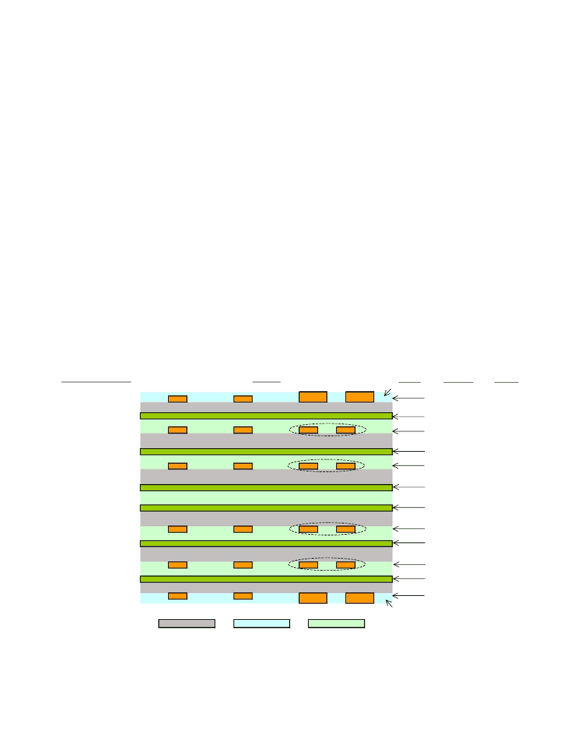
Line Card and Test Card Layer Stackups
The stackups of the Test and Line Cards are presented in this paper to document the standard design practice used in the card layout and
fabrication. Figure 6
and Figure 7
detail the Test Card and Line Card stackups, respectively. The gigabit differential nets of the Test Card
and Line Card were designed to be the same. The length of the traces in the Test Card emulated the lengths seen on the Line Card.
The major difference between the Line and Test Card stackups is the addition of power planes to the Line Card. The Test Card has thicker
dielectric material between layers 6 and 7 to account for the missing plane layers and maintain the same overall card thickness.
Figure 6. WarpLink Test Card Layer Stackup
Dielectric
Solder Mask
Metal weight
Thickness
(mils)
L1
SE Signal / Pad
1 oz. (plated from 0.5 oz.)
1.3
5
0.6
5
0.6
D6
L2
Gnd plane
0.5 oz.
D5
L3
SE Signal / ECD signal
0.5 oz.
D4
5
L4
Gnd plane
0.5 oz.
0.6
5
0.6
D3
L5
SE Signal / ECD signal
0.5 oz.
D2
5
L6
Gnd plane
0.5 oz.
0.6
D1
20
L7
Gnd plane
0.5 oz.
0.6
D2
5
L8
SE Signal / ECD signal
0.5 oz.
0.6
5
0.6
D3
L9
Gnd plane
0.5 oz.
D4
5
L10
SE Signal / ECD signal
0.6
5
0.6
5
1.3
D5
L11
Gnd plane
0.5 oz.
D6
L12
SE Signal / Pad
1 oz. (plated from 0.5 oz.)
Solder Mask
78.6
S = 20mils
GND
Wse=4.5mils
Wdiff
=4mils
Wdiff
=4mils
S = 20mils
S = 20mils
Wdiff
=4mils
5.5 mils
Wdiff
=4mils
Wdiff
=4mils
S = 20mils
S = 20mils
Wse=4.5mils
Wse=4.5mils
Wdiff
=4mils
GND
Wdiff
=4mils
GND
Wse=4.5mils
GND
Wse=4.5mils
Wdiff
=4mils
Sdiff =
5.5 mils
Sdiff =
Pad
S=20mils
Layer Stack
Wtop = 6.5 mils
Wtop = 6.5 mils
Pad
Wse=4.5mils
S=20mils
S = 20mils
S = 20mils
Wse=4.5mils
Wse=4.5mils
Sdiff =
5.5 mils
tan(
δ
)= 0.021
Sdiff =
5.5 mils
GND
S = 20mils
ε
r
= 4.5
FR-4
Pad
S=20mils
Layer number / Description
Total Thickness (pad to pad) =
Pre-Preg
Solder mask
Core
Pad
Wtop = 6.5 mils
Wtop = 6.5 mils
S=20mils
F
Freescale Semiconductor, Inc.
n
.
相關(guān)PDF資料 |
PDF描述 |
|---|---|
| BR200A | TRANSISTOR | BJT | NPN | 50V V(BR)CEO | 20A I(C) | TO-210AC |
| BR200B | TRANSISTOR | BJT | NPN | 50V V(BR)CEO | 20A I(C) | TO-210AC |
| BR201A | TRANSISTOR | BJT | NPN | 75V V(BR)CEO | 20A I(C) | TO-210AC |
| BR201B | TRANSISTOR | BJT | NPN | 75V V(BR)CEO | 20A I(C) | TO-210AC |
| BR211-140AMO | SINGLE BIDIRECTIONAL BREAKOVER DIODE|157V V(BO) MAX|1A I(S)|SOD-84 |
相關(guān)代理商/技術(shù)參數(shù) |
參數(shù)描述 |
|---|---|
| BR158 | 功能描述:橋式整流器 15A 800V RoHS:否 制造商:Vishay 產(chǎn)品:Single Phase Bridge 峰值反向電壓:1000 V 最大 RMS 反向電壓: 正向連續(xù)電流:4.5 A 最大浪涌電流:450 A 正向電壓下降:1 V 最大反向漏泄電流:10 uA 功率耗散: 最大工作溫度:+ 150 C 長度:30.3 mm 寬度:4.1 mm 高度:20.3 mm 安裝風(fēng)格:Through Hole 封裝 / 箱體:SIP-4 封裝:Tube |
| BR158L | 制造商:GOOD-ARK 制造商全稱:GOOD-ARK Electronics 功能描述:SILICON BRIDGE RECTIFIERS |
| BR158W | 功能描述:橋式整流器 15A 800V Wire Lds RoHS:否 制造商:Vishay 產(chǎn)品:Single Phase Bridge 峰值反向電壓:1000 V 最大 RMS 反向電壓: 正向連續(xù)電流:4.5 A 最大浪涌電流:450 A 正向電壓下降:1 V 最大反向漏泄電流:10 uA 功率耗散: 最大工作溫度:+ 150 C 長度:30.3 mm 寬度:4.1 mm 高度:20.3 mm 安裝風(fēng)格:Through Hole 封裝 / 箱體:SIP-4 封裝:Tube |
| BR15A | 制造商:Cooper Wiring Devices 功能描述: |
| BR15A601 | 制造商:Veeder-Root Company 功能描述: |
發(fā)布緊急采購,3分鐘左右您將得到回復(fù)。