- 您現(xiàn)在的位置:買賣IC網(wǎng) > PDF目錄374047 > ADV7344BSTZ (ANALOG DEVICES INC) Multiformat Video Encoder Six 14-Bit Noise Shaped Video DACs PDF資料下載
參數(shù)資料
| 型號(hào): | ADV7344BSTZ |
| 廠商: | ANALOG DEVICES INC |
| 元件分類: | DAC |
| 英文描述: | Multiformat Video Encoder Six 14-Bit Noise Shaped Video DACs |
| 中文描述: | SERIAL INPUT LOADING, 14-BIT DAC, PQFP64 |
| 封裝: | ROHS COMPLIANT, MS-026BCD, LQFP-64 |
| 文件頁數(shù): | 65/88頁 |
| 文件大?。?/td> | 1078K |
| 代理商: | ADV7344BSTZ |
第1頁第2頁第3頁第4頁第5頁第6頁第7頁第8頁第9頁第10頁第11頁第12頁第13頁第14頁第15頁第16頁第17頁第18頁第19頁第20頁第21頁第22頁第23頁第24頁第25頁第26頁第27頁第28頁第29頁第30頁第31頁第32頁第33頁第34頁第35頁第36頁第37頁第38頁第39頁第40頁第41頁第42頁第43頁第44頁第45頁第46頁第47頁第48頁第49頁第50頁第51頁第52頁第53頁第54頁第55頁第56頁第57頁第58頁第59頁第60頁第61頁第62頁第63頁第64頁當(dāng)前第65頁第66頁第67頁第68頁第69頁第70頁第71頁第72頁第73頁第74頁第75頁第76頁第77頁第78頁第79頁第80頁第81頁第82頁第83頁第84頁第85頁第86頁第87頁第88頁
ADV7344
PRINTED CIRCUIT BOARD LAYOUT AND DESIGN
DAC CONFIGURATIONS
The ADV7344 contains six DACs. All six DACs can be
configured to operate in low drive mode. Low drive mode is
defined as 4.33 mA full-scale current into a 300 Ω load, R
L
.
DAC 1, DAC 2, and DAC 3 can also be configured to operate in
full-drive mode. Full-drive mode is defined as 34.7 mA full-
scale current into a 37.5 Ω load, R
L
. Full-drive is the recommended
mode of operation for DAC 1, DAC 2, and DAC 3.
The ADV7344 contains two R
SET
pins. A resistor connected
between the R
SET1
pin and AGND is used to control the full-
scale output current and, therefore, the DAC output voltage
levels of DAC 1, DAC 2, and DAC 3. For low drive operation,
R
SET1
must have a value of 4.12 kΩ, and R
L
must have a value of
300 Ω.
For full-drive operation, R
SET1
must have a value of 510 Ω,
and R
L
must have a value of 37.5 Ω.
A resistor connected between the R
SET2
pin and AGND is used
to control the full-scale output current and, therefore, the DAC
output voltage levels of DAC 4, DAC 5, and DAC 6. R
SET2
must
have a value of 4.12 kΩ, and R
L
must have a value of 300 Ω (that
is, low drive operation only).
The resistors connected to the R
SET1
and R
SET2
pins should have a
1% tolerance.
The ADV7344 contains two compensation pins, COMP1 and
COMP2. A 2.2 nF compensation capacitor should be connected
from each of these pins to V
AA
.
VOLTAGE REFERENCE
The ADV7344 contains an on-chip voltage reference that can be
used as a board-level voltage reference via the V
REF
pin.
Alternatively, the ADV7344 can be used with an external
voltage reference by connecting the reference source to the V
REF
pin. For optimal performance, an external voltage reference
such as the AD1580 should be used with the ADV7344. If an
external voltage reference is not used, a 0.1 μF capacitor should
be connected from the V
REF
pin to V
AA
.
VIDEO OUTPUT BUFFER AND OPTIONAL
OUTPUT FILTER
An output buffer is necessary on any DAC that operates in low
drive mode (R
SET
= 4.12 kΩ, R
L
= 300 Ω). Analog Devices, Inc.
produces a range of op amps suitable for this application, for
example, the AD8061. For more information about line driver
buffering circuits, see the relevant op amp data sheet.
An optional reconstruction (anti-imaging) low-pass filter (LPF)
may be required on the ADV7344 DAC outputs if the ADV7344
is connected to a device that requires this filtering. The filter
specifications vary with the application. The use of 16× (SD), 8×
(ED), or 4× (HD) oversampling can remove the requirement for
a reconstruction filter altogether.
Rev. 0 | Page 65 of 88
For applications requiring an output buffer and reconstruction
filter, the ADA4430-1, ADA4411-3, and ADA4410-6 integrated
video filter buffers should be considered.
Table 53. ADV7344 Output Rates
Input Mode
(0x01, Bits[6:4])
SD Only
PLL Control
(0x00, Bit 1)
Off
On
Off
On
Off
On
Output Rate
(MHz)
27
216
27
216
74.25
297
(2x)
(16x)
(1x)
(8x)
(1x)
(4x)
ED Only
HD Only
Table 54. Output Filter Requirements
Application
SD
SD
ED
ED
HD
HD
Oversampling
2×
16×
1×
8×
1×
4×
Cutoff
Frequency
(MHz)
>6.5
>6.5
>12.5
>12.5
>30
>30
Attenuation
–50 dB @ (MHz)
20.5
209.5
14.5
203.5
44.25
267
560
600
22pF
600
DAC
OUTPUT
75
BNC
OUTPUT
10μH
560
3
4
1
0
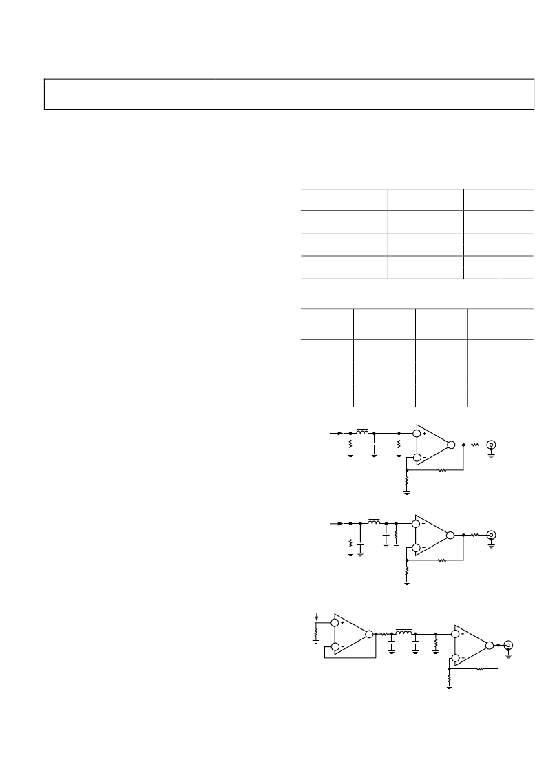
Figure 84. Example of Output Filter for SD, 16× Oversampling
560
6.8pF
600
6.8pF
600
DAC
OUTPUT
75
BNC
OUTPUT
4.7μH
560
3
4
1
0
Figure 85. Example of Output Filter for ED, 8× Oversampling
DAC
OUTPUT
390nH
33pF
33pF
75
500
300
75
BNC
OUTPUT
500
3
4
1
3
4
1
0
Figure 86. Example of Output Filter for HD, 4× Oversampling
相關(guān)PDF資料 |
PDF描述 |
|---|---|
| ADV7390 | Low Power, Chip Scale 10-Bit SD/HD Video Encoder |
| ADV7390BCPZ | Low Power, Chip Scale 10-Bit SD/HD Video Encoder |
| ADV7390BCPZ-REEL | Low Power, Chip Scale 10-Bit SD/HD Video Encoder |
| ADV7390EBZ | Low Power, Chip Scale 10-Bit SD/HD Video Encoder |
| ADV7391 | Low Power, Chip Scale 10-Bit SD/HD Video Encoder |
相關(guān)代理商/技術(shù)參數(shù) |
參數(shù)描述 |
|---|---|
| ADV73505501 | 制造商:LG Corporation 功能描述:Frame Assembly |
| ADV73506801 | 制造商:LG Corporation 功能描述:Frame Assembly |
| ADV73625610 | 制造商:LG Corporation 功能描述:Frame Assembly |
| ADV73625613 | 制造商:LG Corporation 功能描述:Frame Assembly |
| ADV73625616 | 制造商:LG Corporation 功能描述:Frame Assembly |
發(fā)布緊急采購,3分鐘左右您將得到回復(fù)。