- 您現(xiàn)在的位置:買賣IC網(wǎng) > PDF目錄374047 > ADV7344BSTZ (ANALOG DEVICES INC) Multiformat Video Encoder Six 14-Bit Noise Shaped Video DACs PDF資料下載
參數(shù)資料
| 型號(hào): | ADV7344BSTZ |
| 廠商: | ANALOG DEVICES INC |
| 元件分類: | DAC |
| 英文描述: | Multiformat Video Encoder Six 14-Bit Noise Shaped Video DACs |
| 中文描述: | SERIAL INPUT LOADING, 14-BIT DAC, PQFP64 |
| 封裝: | ROHS COMPLIANT, MS-026BCD, LQFP-64 |
| 文件頁數(shù): | 50/88頁 |
| 文件大小: | 1078K |
| 代理商: | ADV7344BSTZ |
第1頁第2頁第3頁第4頁第5頁第6頁第7頁第8頁第9頁第10頁第11頁第12頁第13頁第14頁第15頁第16頁第17頁第18頁第19頁第20頁第21頁第22頁第23頁第24頁第25頁第26頁第27頁第28頁第29頁第30頁第31頁第32頁第33頁第34頁第35頁第36頁第37頁第38頁第39頁第40頁第41頁第42頁第43頁第44頁第45頁第46頁第47頁第48頁第49頁當(dāng)前第50頁第51頁第52頁第53頁第54頁第55頁第56頁第57頁第58頁第59頁第60頁第61頁第62頁第63頁第64頁第65頁第66頁第67頁第68頁第69頁第70頁第71頁第72頁第73頁第74頁第75頁第76頁第77頁第78頁第79頁第80頁第81頁第82頁第83頁第84頁第85頁第86頁第87頁第88頁
ADV7344
Rev. 0 | Page 50 of 88
LCC1
SFL
P19 TO P10
ADV7403
VIDEO
DECODER
CLKIN_A
SFL/MISO
Y9 TO Y0/
S9 TO S0
5
RTC
LOW
128
TIME SLOT 01
13
0
14
21
19
F
SC
PLL INCREMENT
2
VALID
SAMPLE
INVALID
SAMPLE
6768
0
RESET BIT
4
RESERVED
ADV7344
8/LINE
LOCKED
CLOCK
5 BITS
RESERVED
1
FOR EXAMPLE, VCR OR CABLE.
2
F
SC
PLL INCREMENT IS 22 BITS LONG. VALUE LOADED INTO ADV7344 F
DDS REGISTER IS
F
PLL INCREMENTS BITS 21:0 PLUS BITS 0:9 OF SUBCARRIER FREQUENCY REGISTERS.
3
SEQUENCE BIT
PAL: 0 = LINE NORMAL, 1 = LINE INVERTED
NTSC: 0 = NO CHANGE
4
RESET ADV7344 DDS.
5
SELECTED BY SUBADDRESS 0x01, BIT 7.
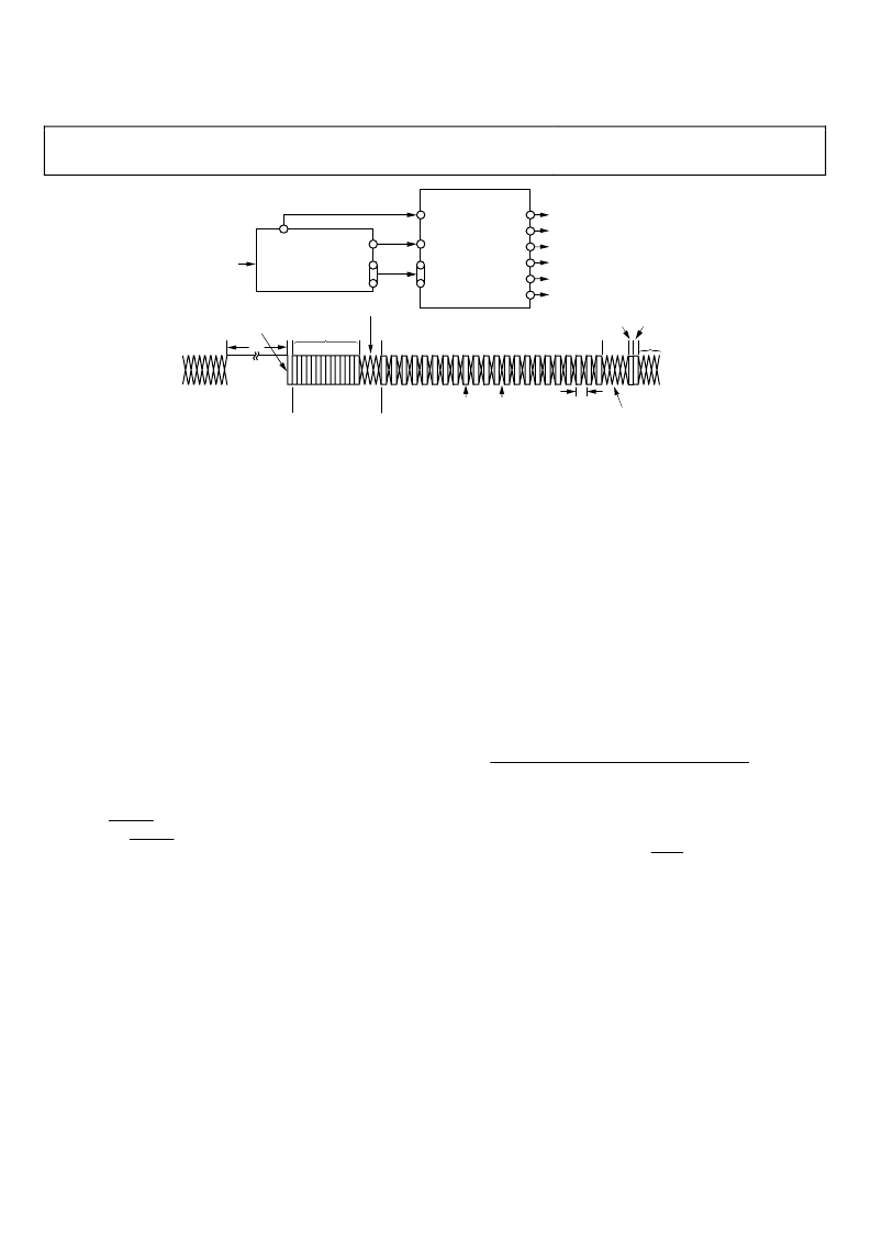
Figure 62. SD Subcarrier Frequency Lock Timing and Connections Diagram (Subaddress 0x84, Bits[2:1] = 11)
COMPOSITE
VIDEO
1
H/L TRANSITION
COUNT START
14 BITS
SUBCARRIER
PHASE
SEQUENCE
BIT
3
DAC 1
DAC 2
DAC 3
DAC 4
DAC 5
DAC 6
4 BITS
RESERVED
0
SD VCR FF/RW SYNC
Subaddress 0x82, Bit 5
In DVD record applications where the encoder is used with a
decoder, the VCR FF/RW sync control bit can be used for
nonstandard input video, that is, in fast forward or rewind modes.
In fast forward mode, the sync information at the start of a new
field in the incoming video usually occurs before the correct
number of lines/fields is reached. In rewind mode, this sync
signal usually occurs after the total number of lines/fields is
reached. Conventionally, this means that the output video has
corrupted field signals because one signal is generated by the
incoming video and another is generated when the internal
line/field counters reach the end of a field.
When the VCR FF/RW sync control is enabled (Subaddress 0x82,
Bit 5), the line/field counters are updated according to the
incoming VSYNC signal and when the analog output matches
the incoming VSYNC signal.
This control is available in all slave-timing modes except Slave
Mode 0.
VERTICAL BLANKING INTERVAL
Subaddress 0x31, Bit 4; Subaddress 0x83, Bit 4
The ADV7344 is able to accept input data that contains VBI
data (such as CGMS, WSS, VITS) in SD, ED, and HD modes.
If VBI is disabled (Subaddress 0x31, Bit 4 for ED/HD;
Subaddress 0x83, Bit 4 for SD), VBI data is not present at the
output and the entire VBI is blanked. These control bits are
valid in all master and slave timing modes.
For the SMPTE 293M (525p) standard, VBI data can be
inserted on Line 13 to Line 42 of each frame, or on Line 6 to
Line 43 for the ITU-R BT.1358 (625p) standard.
VBI data can be present on Line 10 to Line 20 for NTSC and on
Line 7 to Line 22 for PAL.
In SD Timing Mode 0 (slave option), if VBI is enabled, the
blanking bit in the EAV/SAV code is overwritten. It is possible
to use VBI in this timing mode as well.
If CGMS is enabled and VBI is disabled, the CGMS data is
nevertheless available at the output.
SD SUBCARRIER FREQUENCY REGISTERS
Subaddress 0x8C to Subaddress 0x8F
Four 8-bit registers are used to set up the subcarrier frequency.
The value of these registers is calculated using:
Register
Frequency
Subcarrier
32
2
MHz
27
×
=
in
line
video
one
in
cycles
clk
of
Number
line
video
one
periods
subcarrier
of
Number
where the sum is rounded to the nearest integer. For example, in
NTSC mode:
569408543
2
1716
5
227
32
=
×
=
Value
Register
Subcarrier
where:
Subcarrier Register Value
= 569408543d = 0×21F07C1F
SD F
SC
Register 0: 0x1F
SD F
SC
Register 1: 0x7C
SD F
SC
Register 2: 0xF0
SD F
SC
Register 3: 0x21
Programming the F
SC
The subcarrier frequency register value is divided into four F
SC
registers as shown in the previous example. The four subcarrier
frequency registers must be updated sequentially, starting with
Subcarrier Frequency Register 0 and ending with Subcarrier
Frequency Register 3. The subcarrier frequency updates only
after the last subcarrier frequency register byte has been
received by the ADV7344.
相關(guān)PDF資料 |
PDF描述 |
|---|---|
| ADV7390 | Low Power, Chip Scale 10-Bit SD/HD Video Encoder |
| ADV7390BCPZ | Low Power, Chip Scale 10-Bit SD/HD Video Encoder |
| ADV7390BCPZ-REEL | Low Power, Chip Scale 10-Bit SD/HD Video Encoder |
| ADV7390EBZ | Low Power, Chip Scale 10-Bit SD/HD Video Encoder |
| ADV7391 | Low Power, Chip Scale 10-Bit SD/HD Video Encoder |
相關(guān)代理商/技術(shù)參數(shù) |
參數(shù)描述 |
|---|---|
| ADV73505501 | 制造商:LG Corporation 功能描述:Frame Assembly |
| ADV73506801 | 制造商:LG Corporation 功能描述:Frame Assembly |
| ADV73625610 | 制造商:LG Corporation 功能描述:Frame Assembly |
| ADV73625613 | 制造商:LG Corporation 功能描述:Frame Assembly |
| ADV73625616 | 制造商:LG Corporation 功能描述:Frame Assembly |
發(fā)布緊急采購,3分鐘左右您將得到回復(fù)。