- 您現(xiàn)在的位置:買(mǎi)賣(mài)IC網(wǎng) > PDF目錄223307 > ADE7878ACPZ (ANALOG DEVICES INC) Poly Phase Multifunction Energy Metering IC With Total And Fundamental Powers, No Of Pins: 40, Temperature Range: Ind PDF資料下載
參數(shù)資料
| 型號(hào): | ADE7878ACPZ |
| 廠商: | ANALOG DEVICES INC |
| 元件分類: | 模擬信號(hào)調(diào)理 |
| 英文描述: | Poly Phase Multifunction Energy Metering IC With Total And Fundamental Powers, No Of Pins: 40, Temperature Range: Ind |
| 中文描述: | SPECIALTY ANALOG CIRCUIT, QCC40 |
| 封裝: | 6 X 6 MM, ROHS COMPLIANT, MO-220WJJD, LFCSP-40 |
| 文件頁(yè)數(shù): | 7/96頁(yè) |
| 文件大?。?/td> | 1096K |
| 代理商: | ADE7878ACPZ |
第1頁(yè)第2頁(yè)第3頁(yè)第4頁(yè)第5頁(yè)第6頁(yè)當(dāng)前第7頁(yè)第8頁(yè)第9頁(yè)第10頁(yè)第11頁(yè)第12頁(yè)第13頁(yè)第14頁(yè)第15頁(yè)第16頁(yè)第17頁(yè)第18頁(yè)第19頁(yè)第20頁(yè)第21頁(yè)第22頁(yè)第23頁(yè)第24頁(yè)第25頁(yè)第26頁(yè)第27頁(yè)第28頁(yè)第29頁(yè)第30頁(yè)第31頁(yè)第32頁(yè)第33頁(yè)第34頁(yè)第35頁(yè)第36頁(yè)第37頁(yè)第38頁(yè)第39頁(yè)第40頁(yè)第41頁(yè)第42頁(yè)第43頁(yè)第44頁(yè)第45頁(yè)第46頁(yè)第47頁(yè)第48頁(yè)第49頁(yè)第50頁(yè)第51頁(yè)第52頁(yè)第53頁(yè)第54頁(yè)第55頁(yè)第56頁(yè)第57頁(yè)第58頁(yè)第59頁(yè)第60頁(yè)第61頁(yè)第62頁(yè)第63頁(yè)第64頁(yè)第65頁(yè)第66頁(yè)第67頁(yè)第68頁(yè)第69頁(yè)第70頁(yè)第71頁(yè)第72頁(yè)第73頁(yè)第74頁(yè)第75頁(yè)第76頁(yè)第77頁(yè)第78頁(yè)第79頁(yè)第80頁(yè)第81頁(yè)第82頁(yè)第83頁(yè)第84頁(yè)第85頁(yè)第86頁(yè)第87頁(yè)第88頁(yè)第89頁(yè)第90頁(yè)第91頁(yè)第92頁(yè)第93頁(yè)第94頁(yè)第95頁(yè)第96頁(yè)
ADE7854/ADE7858/ADE7868/ADE7878
Rev. E | Page 15 of 96
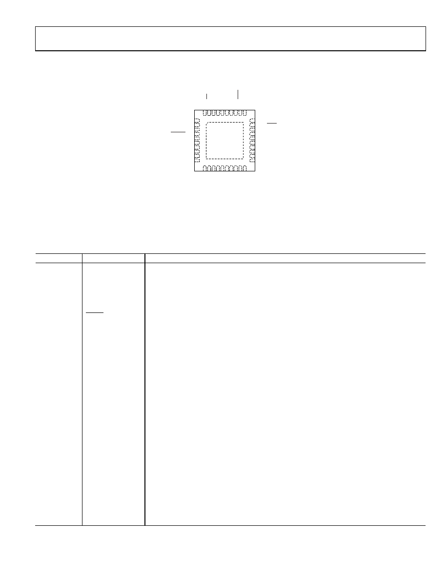
PIN CONFIGURATION AND FUNCTION DESCRIPTIONS
NOTES
1. NC = NO CONNECT.
2. CREATE A SIMILAR PAD ON THE PCB UNDER THE
EXPOSED PAD. SOLDER THE EXPOSED PAD TO
THE PAD ON THE PCB TO CONFER MECHANICAL
STRENGTH TO THE PACKAGE. DO NOT CONNECT
THE PADS TO AGND.
11
N
C
12
IB
N
13
IC
P
15
IN
P
17
R
E
F
IN
/O
U
T
16
IN
N
18
V
N
19
V
C
P
20
N
C
14
IC
N
NC
PM0
PM1
RESET
DVDD
DGND
IAP
IAN
IBP
NC
VAP
AVDD
AGND
VDD
CLKIN
CLKOUT
IRQ0
NC
VBP
NC
33
C
F
1
34
C
F
2
35
C
F
3/
H
S
C
L
K
36
S
C
L
K
/S
C
L
37
M
IS
O
/H
S
D
38
M
O
S
I/
S
D
A
39
S
/H
S
A
40
N
C
32
IR
Q
1
31
N
C
08
51
0-
1
06
1
2
3
4
5
6
7
8
9
10
23
24
25
26
27
28
29
30
22
21
ADE78xx
TOP VIEW
(Not to Scale)
Figure 9. Pin Configuration
Table 8. Pin Function Descriptions
Pin No.
Mnemonic
Description
1, 10, 11, 20,
21, 30, 31, 40
NC
No Connect. These pins are not connected internally.
2
PM0
Power Mode Pin 0. This pin, combined with PM1, defines the power mode of the
ADE7854/ADE7858/ADE7868/ADE7878, as described in Table 9.
3
PM1
Power Mode Pin 1. This pin defines the power mode of the ADE7854/ADE7858/ADE7868/ADE7878
when combined with PM0, as described in Table 9.
4
RESET
Reset Input, Active Low. In PSM0 mode, this pin should stay low for at least 10 μs to trigger a
hardware reset.
5
DVDD
This pin provides access to the on-chip 2.5 V digital LDO. Do not connect any external active
circuitry to this pin. Decouple this pin with a 4.7 μF capacitor in parallel with a ceramic 220 nF
capacitor.
6
DGND
Ground Reference. This pin provides the ground reference for the digital circuitry.
7, 8
IAP, IAN
Analog Inputs for Current Channel A. This channel is used with the current transducers and is
referenced in this document as Current Channel A. These inputs are fully differential voltage inputs
with a maximum differential level of ±0.5 V. This channel also has an internal PGA equal to the ones
on Channel B and Channel C.
9, 12
IBP, IBN
Analog Inputs for Current Channel B. This channel is used with the current transducers and is
referenced in this document as Current Channel B. These inputs are fully differential voltage inputs
with a maximum differential level of ±0.5 V. This channel also has an internal PGA equal to the ones
on Channel C and Channel A.
13, 14
ICP, ICN
Analog Inputs for Current Channel C. This channel is used with the current transducers and is
referenced in this document as Current Channel C. These inputs are fully differential voltage inputs
with a maximum differential level of ±0.5 V. This channel also has an internal PGA equal to the ones
on Channel A and Channel B.
15, 16
INP, INN
Analog Inputs for Neutral Current Channel N. This channel is used with the current transducers and
is referenced in this document as Current Channel N. These inputs are fully differential voltage
inputs with a maximum differential level of ±0.5 V. This channel also has an internal PGA, different
from the ones found on the A, B, and C channels. The neutral current channel is available in the
ADE7878 and ADE7868. In the ADE7858 and ADE7854, connect these pins to AGND.
17
REFIN/OUT
This pin provides access to the on-chip voltage reference. The on-chip reference has a nominal
value of 1.2 V. An external reference source with 1.2 V ± 8% can also be connected at this pin. In
either case, decouple this pin to AGND with a 4.7 μF capacitor in parallel with a ceramic 100 nF
capacitor. After reset, the on-chip reference is enabled.
相關(guān)PDF資料 |
PDF描述 |
|---|---|
| ADE7878ACPZ-RL | Poly Phase Multifunction Energy Metering IC With Total And Fundamental Powers, No Of Pins: 40, Temperature Range: Ind |
| ADG529FTQ | 4-CHANNEL, DIFFERENTIAL MULTIPLEXER, CDIP18 |
| ADJ24006 | POWER/SIGNAL RELAY, SPST, LATCHED, 0.042A (COIL), 6VDC (COIL), 250mW (COIL), THROUGH HOLE-STRAIGHT MOUNT |
| ADJ24012 | POWER/SIGNAL RELAY, SPST, LATCHED, 0.021A (COIL), 12VDC (COIL), 250mW (COIL), THROUGH HOLE-STRAIGHT MOUNT |
| ADJ24024 | POWER/SIGNAL RELAY, SPST, LATCHED, 0.01A (COIL), 24VDC (COIL), 250mW (COIL), THROUGH HOLE-STRAIGHT MOUNT |
相關(guān)代理商/技術(shù)參數(shù) |
參數(shù)描述 |
|---|---|
| ADE7878ACPZ | 制造商:Analog Devices 功能描述:IC MULTIFUNCTION ENERGY METERING LFCSP40 |
| ADE7878ACPZ-RL | 功能描述:IC ENERGY METERING 3PH 40LFCSP RoHS:是 類別:集成電路 (IC) >> PMIC - 能量測(cè)量 系列:- 產(chǎn)品培訓(xùn)模塊:Lead (SnPb) Finish for COTS Obsolescence Mitigation Program 標(biāo)準(zhǔn)包裝:2,500 系列:* |
| ADE7878XCPZ | 制造商:Analog Devices 功能描述:POLY PHASE MULTIFUNCTION ENERGY METERING IC WITH TOTAL - Bulk |
| ADE7880 | 制造商:Analog Devices 功能描述:BOARD EVAL ENERGY METER ADE |
| ADE7880ACPZ | 功能描述:IC ENERGY METERING 3PH 40LFCSP RoHS:是 類別:集成電路 (IC) >> PMIC - 能量測(cè)量 系列:- 產(chǎn)品培訓(xùn)模塊:Lead (SnPb) Finish for COTS Obsolescence Mitigation Program 標(biāo)準(zhǔn)包裝:2,500 系列:* |
發(fā)布緊急采購(gòu),3分鐘左右您將得到回復(fù)。