- 您現(xiàn)在的位置:買賣IC網(wǎng) > PDF目錄223307 > ADE7878ACPZ (ANALOG DEVICES INC) Poly Phase Multifunction Energy Metering IC With Total And Fundamental Powers, No Of Pins: 40, Temperature Range: Ind PDF資料下載
參數(shù)資料
| 型號: | ADE7878ACPZ |
| 廠商: | ANALOG DEVICES INC |
| 元件分類: | 模擬信號調(diào)理 |
| 英文描述: | Poly Phase Multifunction Energy Metering IC With Total And Fundamental Powers, No Of Pins: 40, Temperature Range: Ind |
| 中文描述: | SPECIALTY ANALOG CIRCUIT, QCC40 |
| 封裝: | 6 X 6 MM, ROHS COMPLIANT, MO-220WJJD, LFCSP-40 |
| 文件頁數(shù): | 25/96頁 |
| 文件大小: | 1096K |
| 代理商: | ADE7878ACPZ |
第1頁第2頁第3頁第4頁第5頁第6頁第7頁第8頁第9頁第10頁第11頁第12頁第13頁第14頁第15頁第16頁第17頁第18頁第19頁第20頁第21頁第22頁第23頁第24頁當前第25頁第26頁第27頁第28頁第29頁第30頁第31頁第32頁第33頁第34頁第35頁第36頁第37頁第38頁第39頁第40頁第41頁第42頁第43頁第44頁第45頁第46頁第47頁第48頁第49頁第50頁第51頁第52頁第53頁第54頁第55頁第56頁第57頁第58頁第59頁第60頁第61頁第62頁第63頁第64頁第65頁第66頁第67頁第68頁第69頁第70頁第71頁第72頁第73頁第74頁第75頁第76頁第77頁第78頁第79頁第80頁第81頁第82頁第83頁第84頁第85頁第86頁第87頁第88頁第89頁第90頁第91頁第92頁第93頁第94頁第95頁第96頁
ADE7854/ADE7858/ADE7868/ADE7878
Rev. E | Page 31 of 96
Voltage Waveform Gain Registers
There is a multiplier in the signal path of each phase voltage.
The voltage waveform can be changed by ±100% by writing
a corresponding twos complement number to the 24-bit signed
current waveform gain registers (AVGAIN, BVGAIN, and
CVGAIN). For example, if 0x400000 is written to those registers,
the ADC output is scaled up by 50%. To scale the input by 50%,
write 0xC00000 to the registers. Equation 4 describes mathe-
matically the function of the current waveform gain registers.
Voltage Waveform =
+
×
23
2
1
Register
Gain
Voltage
of
Content
Output
ADC
(4)
Changing the content of the AVGAIN, BVGAIN, and CVGAIN
registers affects all calculations based on its voltage; that is, it
affects the corresponding phase active/reactive/apparent energy
and voltage rms calculation. In addition, waveform samples are
scaled accordingly.
As stated in the Current Waveform Gain Registers section, the
serial ports of the ADE78xx work on 32-, 16-, or 8-bit words,
and the DSP works on 28 bits. As presented in Figure 33, the
AVGAIN, BVGAIN, and CVGAIN registers are accessed as
32-bit registers with four MSBs padded with 0s and sign
extended to 28 bits.
Voltage Channel HPF
As explained in the Current Channel HPF section, the ADC
outputs can contain a dc offset that can create errors in power
and rms calculations. HPFs are placed in the signal path of the
phase voltages, similar to the ones in the current channels. The
HPFDIS register can enable or disable the filters. See the
Current Channel HPF section for more details.
Voltage Channel Sampling
The waveform samples of the voltage channel are taken at the
output of HPF and stored into VAWV, VBWV, and VCWV
24-bit signed registers at a rate of 8 kSPS. All power and rms
calculations remain uninterrupted during this process. Bit 17
(DREADY) in the STATUS0 register is set when the VAWV,
VBWV, and VCWV registers are available to be read using the
I2C or SPI serial port. Setting Bit 17 (DREADY) in the MASK0
register enables an interrupt to be set when the DREADY flag is
set. See the Digital Signal Processor section for more details on
Bit DREADY.
As stated in the Current Waveform Gain Registers section, the
serial ports of the ADE78xx work on 32-, 16-, or 8-bit words.
Similar to registers presented in Figure 35, the VAWV, VBWV,
and VCWV 24-bit signed registers are transmitted sign
extended to 32 bits.
The ADE7854/ADE7858/ADE7868/ADE7878 each contain an
HSDC port especially designed to provide fast access to the
waveform sample registers. See the HSDC Interface section for
more details.
CHANGING PHASE VOLTAGE DATAPATH
The ADE7854/ADE7858/ADE7868/ADE7878 can direct one
phase voltage input to the computational datapath of another
phase. For example, Phase A voltage can be introduced in the
Phase B computational datapath, which means all powers
computed by the ADE78xx in Phase B are based on Phase A
voltage and Phase B current.
Bits[9:8] (VTOIA[1:0]) of the CONFIG register manage the
Phase A voltage measured at the VA pin. If VTOIA[1:0] = 00
(default value), the voltage is directed to the Phase A computa-
tional datapath. If VTOIA[1:0] = 01, the voltage is directed to
the Phase B path. If VTOIA[1:0] = 10, the voltage is directed to the
Phase C path. If VTOIA[1:0] = 11, the ADE7878 behaves as if
VTOIA[1:0] = 00.
Bits[11:10] (VTOIB[1:0]) of the CONFIG register manage the
Phase B voltage measured at the VB pin. If VTOIB[1:0] = 00
(default value), the voltage is directed to the Phase B computa-
tional datapath. If VTOIB[1:0] = 01, the voltage is directed to
the Phase C path. If VTOIB[1:0] = 10, the voltage is directed to
the Phase A path. If VTOIB[1:0] = 11, the ADE78xx behaves
as if VTOIB[1:0] = 00.
Bits[13:12] (VTOIC[1:0]) of the CONFIG register manage the
Phase C voltage measured at the VC pin. If VTOIC[1:0] = 00
(default value), the voltage is directed to Phase C computational
datapath, if VTOIC[1:0] = 01, the voltage is directed to the
Phase A path. If VTOIC[1:0] = 10, the voltage is directed to the
Phase B path. If VTOIC[1:0] = 11, the ADE78xx behaves as if
VTOIC[1:0] = 00.
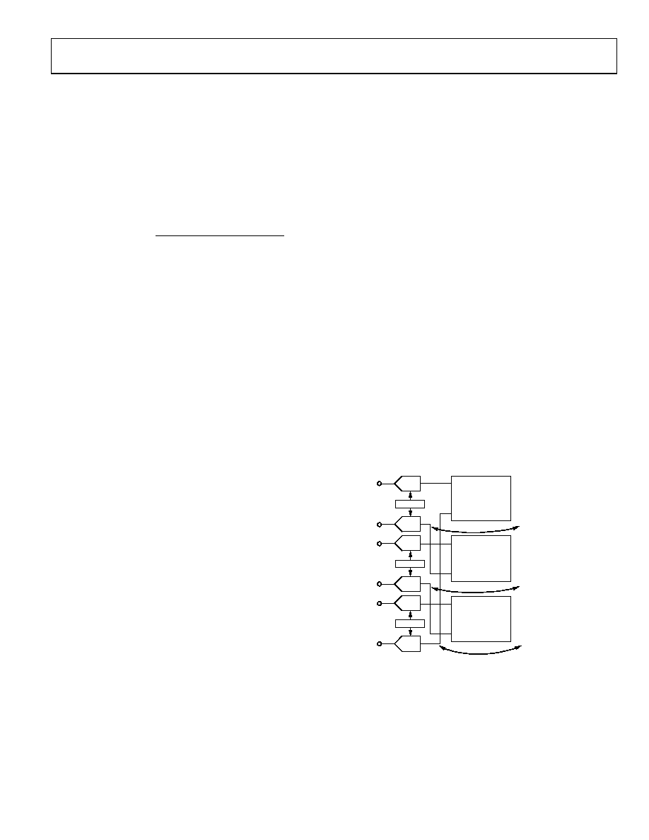
IA
VA
IB
VB
IC
VC
PHASE A
COMPUTATIONAL
DATAPATH
PHASE B
COMPUTATIONAL
DATAPATH
PHASE C
COMPUTATIONAL
DATAPATH
VTOIA[1:0] = 01,
PHASE A VOLTAGE
DIRECTED
TO PHASE B
VTOIB[1:0] = 01,
PHASE B VOLTAGE
DIRECTED
TO PHASE C
VTOIC[1:0] = 01,
PHASE C VOLTAGE
DIRECTED
TO PHASE A
CPHCAL
BPHCAL
APHCAL
08
51
0-
02
6
Figure 40. Phase Voltages Used in Different Datapaths
Figure 40 presents the case in which Phase A voltage is used in
the Phase B datapath, Phase B voltage is used in the Phase C
datapath, and Phase C voltage is used in the Phase A datapath.
相關(guān)PDF資料 |
PDF描述 |
|---|---|
| ADE7878ACPZ-RL | Poly Phase Multifunction Energy Metering IC With Total And Fundamental Powers, No Of Pins: 40, Temperature Range: Ind |
| ADG529FTQ | 4-CHANNEL, DIFFERENTIAL MULTIPLEXER, CDIP18 |
| ADJ24006 | POWER/SIGNAL RELAY, SPST, LATCHED, 0.042A (COIL), 6VDC (COIL), 250mW (COIL), THROUGH HOLE-STRAIGHT MOUNT |
| ADJ24012 | POWER/SIGNAL RELAY, SPST, LATCHED, 0.021A (COIL), 12VDC (COIL), 250mW (COIL), THROUGH HOLE-STRAIGHT MOUNT |
| ADJ24024 | POWER/SIGNAL RELAY, SPST, LATCHED, 0.01A (COIL), 24VDC (COIL), 250mW (COIL), THROUGH HOLE-STRAIGHT MOUNT |
相關(guān)代理商/技術(shù)參數(shù) |
參數(shù)描述 |
|---|---|
| ADE7878ACPZ | 制造商:Analog Devices 功能描述:IC MULTIFUNCTION ENERGY METERING LFCSP40 |
| ADE7878ACPZ-RL | 功能描述:IC ENERGY METERING 3PH 40LFCSP RoHS:是 類別:集成電路 (IC) >> PMIC - 能量測量 系列:- 產(chǎn)品培訓(xùn)模塊:Lead (SnPb) Finish for COTS Obsolescence Mitigation Program 標準包裝:2,500 系列:* |
| ADE7878XCPZ | 制造商:Analog Devices 功能描述:POLY PHASE MULTIFUNCTION ENERGY METERING IC WITH TOTAL - Bulk |
| ADE7880 | 制造商:Analog Devices 功能描述:BOARD EVAL ENERGY METER ADE |
| ADE7880ACPZ | 功能描述:IC ENERGY METERING 3PH 40LFCSP RoHS:是 類別:集成電路 (IC) >> PMIC - 能量測量 系列:- 產(chǎn)品培訓(xùn)模塊:Lead (SnPb) Finish for COTS Obsolescence Mitigation Program 標準包裝:2,500 系列:* |
發(fā)布緊急采購,3分鐘左右您將得到回復(fù)。