- 您現(xiàn)在的位置:買賣IC網(wǎng) > PDF目錄2064 > ADAV4601BSTZ (Analog Devices Inc)IC AUDIO CODEC PROCESSOR 80-LQFP PDF資料下載
參數(shù)資料
| 型號(hào): | ADAV4601BSTZ |
| 廠商: | Analog Devices Inc |
| 文件頁(yè)數(shù): | 18/60頁(yè) |
| 文件大小: | 0K |
| 描述: | IC AUDIO CODEC PROCESSOR 80-LQFP |
| 標(biāo)準(zhǔn)包裝: | 1 |
| 系列: | SigmaDSP® |
| 類型: | 音頻處理器 |
| 應(yīng)用: | TV |
| 安裝類型: | 表面貼裝 |
| 封裝/外殼: | 80-LQFP |
| 供應(yīng)商設(shè)備封裝: | 80-LQFP(14x14) |
| 包裝: | 托盤(pán) |
第1頁(yè)第2頁(yè)第3頁(yè)第4頁(yè)第5頁(yè)第6頁(yè)第7頁(yè)第8頁(yè)第9頁(yè)第10頁(yè)第11頁(yè)第12頁(yè)第13頁(yè)第14頁(yè)第15頁(yè)第16頁(yè)第17頁(yè)當(dāng)前第18頁(yè)第19頁(yè)第20頁(yè)第21頁(yè)第22頁(yè)第23頁(yè)第24頁(yè)第25頁(yè)第26頁(yè)第27頁(yè)第28頁(yè)第29頁(yè)第30頁(yè)第31頁(yè)第32頁(yè)第33頁(yè)第34頁(yè)第35頁(yè)第36頁(yè)第37頁(yè)第38頁(yè)第39頁(yè)第40頁(yè)第41頁(yè)第42頁(yè)第43頁(yè)第44頁(yè)第45頁(yè)第46頁(yè)第47頁(yè)第48頁(yè)第49頁(yè)第50頁(yè)第51頁(yè)第52頁(yè)第53頁(yè)第54頁(yè)第55頁(yè)第56頁(yè)第57頁(yè)第58頁(yè)第59頁(yè)第60頁(yè)
ADAV4601
Rev. B | Page 25 of 60
Examples
1000 0000 0000 0000 0000 0000 0000 = 16.0
1110 0000 0000 0000 0000 0000 0000 = 4.0
1111 1000 0000 0000 0000 0000 0000 = 1.0
1111 1110 0000 0000 0000 0000 0000 = 0.25
1111 1111 1111 1111 1111 1111 1111 = (1 LSB below 0.0)
0000 0000 0000 0000 0000 0000 0000 = 0.0
0000 0010 0000 0000 0000 0000 0000 = +0.25
0000 1000 0000 0000 0000 0000 0000 = +1.0
0010 0000 0000 0000 0000 0000 0000 = +4.0
0111 1111 1111 1111 1111 1111 1111 = (+16.0 1 LSB)
The serial port accepts up to 24 bits on the input and is sign-
extended to the full 28 bits of the DSP core. This allows internal
gains of up to 24 dB without internal clipping.
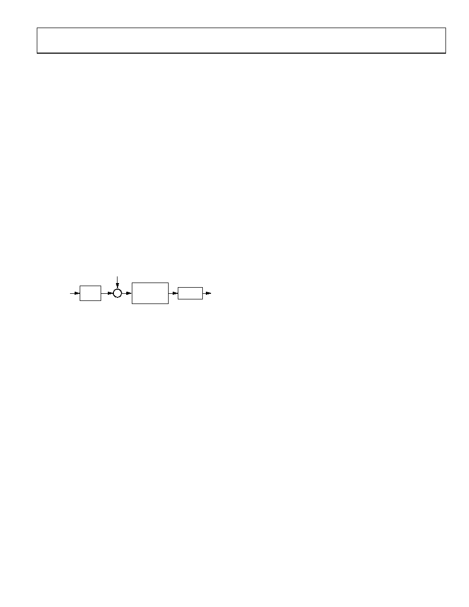
A digital clipper circuit is used between the output of the DSP
core and the DACs or serial port outputs (see Figure 38). This
clips the top four bits of the signal to produce a 24-bit output
with a range of +1.0 (minus 1 LSB) to 1.0. Figure 38 shows
the maximum signal levels at each point in the data flow in
both binary and decibel levels.
4-BIT SIGN EXTENSION
DATA IN
1.23
(0dB)
1.23
(0dB)
1.23
(0dB)
5.23
(24dB)
5.23
(24dB)
SERIAL
PORT
SIGNAL
PROCESSING
(5.23 FORMAT)
DIGITAL
CLIPPER
0
707
0-
1
10
Figure 38. Numeric Precision and Clipping Structure
ROMS AND REGISTERS
The ADAV4601 contains four ROMS: program, instruction,
parameter, and LUT. A default set of ROMs is stored on chip
and is loaded on power-up. A set of ROMs defining a custom
flow can be stored externally on an EEPROM and can be loaded
after power-up.
Program ROM
Program ROM is 42-bits wide and occupies Address 0x1400 to
Address 0x1FFF. This is where the audio flow generated in
SigmaStudio is stored.
Instruction ROM
Instruction ROM is 33-bits wide and occupies Address 0x3000
to Address 0x327F. This is where the application layer register
map is stored.
Parameter ROM
Parameter ROM is 28-bits wide and occupies Address 0x1000 to
Address 0x13FF. Default parameters for default flow and custom
flow are stored here.
LUT ROM
LUT ROM is 28-bits wide and occupies Address 0x4000 to
Address 0x57FF. This contains the parameters for both flows
combined.
SAFE LOADING TO PARAMETER RAM AND
TARGET/SLEW RAM
Up to five safe load registers can be loaded with parameter
RAM address data. The data is transferred to the requested
address when the RAM is idle. It is recommended to use this
method for dynamic updates during run time. For example, a
complete update of one biquad section can occur in one audio
frame. This method is not available for writing to the program
RAM or control registers.
There are ten safe load registers operating in pairs of five, where
five of them store addresses and five of them store data. To safe
load a register, move its address into a safe load address register
and move its data into the corresponding safe load data register. If it
is a parameter RAM, set Bit 4 in Register 0x0200 to 1 to initiate the
safe load. If it is a target/slew RAM, set Bit 5 in Register 0x0200
to 1 to initiate the safe load.
The safe load data registers are located from Address 0x2040 to
Address 0x2044 and are five-bytes wide.
The safe load address registers are located from Address 0x2045 to
Address 0x2049 and are two-bytes wide.
The last five instructions of the program RAM are used for the safe
load process; therefore, the program length should be limited to
2555 cycles (2560 5). It is guaranteed that the safe load occurs
within one LRCLK period (21 μs at fS = 48 kHz) of the initiate
safe transfer bit being set. Safe load only updates those safe load
registers that have been loaded with new data since the last safe
load operation. For example, if only two parameters or target
RAM locations are updated, it is only necessary to load two of
the safe load registers; the other safe load registers are ignored
because they contain old data.
READ/WRITE DATA FORMATS
The read/write formats of the control port are designed to be
byte oriented. This allows easy programming of common micro-
controller chips. To fit into a byte-oriented format, 0s are appended
to the data fields before the MSB to extend the data-word to
eight bits. For example, 28-bit words written to the parameter
RAM are appended with four leading 0s to equal 32 bits (4 bytes);
40-bit words written to the program RAM are not appended
with 0s because they are already a full five bytes. These zero-
padded data fields are appended to a 3-byte field consisting of a
7-bit chip address, a read/write bit, and a 16-bit RAM/register
address. The control port knows how many data bytes to expect
based on the address given in the first three bytes.
The total number of bytes for a single location write command
can vary from five bytes (for a control register write) to eight bytes
(for a program RAM write). Burst mode can be used to fill
contiguous register or RAM locations. A burst mode write begins
by writing the address and data of the first RAM or register
location to be written to. Rather than ending the control port
transaction (by issuing a stop command in I2C mode), as would
be done in a single-address write, the next data-word can be
written immediately without specifying its address.
相關(guān)PDF資料 |
PDF描述 |
|---|---|
| ADAV4622BSTZ | IC AUD PRO ATV/SIF DECODE 80LQFP |
| ADCLK846BCPZ-REEL7 | IC CLK BUFFER 1:6 1.2GHZ 24LFCSP |
| ADCLK854BCPZ | IC CLOCK BUFFER MUX 2:12 48LFCSP |
| ADCLK907BCPZ-WP | IC CLK/DATA BUFF DVR 1:1 16LFCSP |
| ADCLK914BCPZ-WP | IC CLK/DATA BUFF DVR 1:1 16LFCSP |
相關(guān)代理商/技術(shù)參數(shù) |
參數(shù)描述 |
|---|---|
| ADAV4622 | 制造商:AD 制造商全稱:Analog Devices 功能描述:Audio Processor for Advanced TV with Sound IF Demodulator and Stereo Decoder |
| ADAV4622BSTZ | 功能描述:IC AUD PRO ATV/SIF DECODE 80LQFP RoHS:是 類別:集成電路 (IC) >> 線性 - 音頻處理 系列:SigmaDSP® 其它有關(guān)文件:STA321 View All Specifications 標(biāo)準(zhǔn)包裝:1 系列:Sound Terminal™ 類型:音頻處理器 應(yīng)用:數(shù)字音頻 安裝類型:表面貼裝 封裝/外殼:64-LQFP 裸露焊盤(pán) 供應(yīng)商設(shè)備封裝:64-LQFP EP(10x10) 包裝:Digi-Reel® 其它名稱:497-11050-6 |
| ADAV4-KIT-1 | 制造商:Wiebetech 功能描述:Combo Dock Kit #1 for Weibetech Ultradock Series |
| ADAV801 | 制造商:AD 制造商全稱:Analog Devices 功能描述:Audio Codec for Recordable DVD |
| ADAV801AST | 制造商:Analog Devices 功能描述:AUDIO CODEC FOR RECORDABLE DVD - Bulk |
發(fā)布緊急采購(gòu),3分鐘左右您將得到回復(fù)。