- 您現(xiàn)在的位置:買賣IC網(wǎng) > PDF目錄1894 > AD9858BSVZ (Analog Devices Inc)IC DDS DAC 10BIT 1GSPS 100-TQFP PDF資料下載
參數(shù)資料
| 型號: | AD9858BSVZ |
| 廠商: | Analog Devices Inc |
| 文件頁數(shù): | 28/32頁 |
| 文件大?。?/td> | 0K |
| 描述: | IC DDS DAC 10BIT 1GSPS 100-TQFP |
| 產(chǎn)品培訓模塊: | Direct Digital Synthesis Tutorial Series (1 of 7): Introduction Direct Digital Synthesizer Tutorial Series (7 of 7): DDS in Action Direct Digital Synthesis Tutorial Series (3 of 7): Angle to Amplitude Converter Direct Digital Synthesis Tutorial Series (6 of 7): SINC Envelope Correction Direct Digital Synthesis Tutorial Series (4 of 7): Digital-to-Analog Converter Direct Digital Synthesis Tutorial Series (2 of 7): The Accumulator |
| 設計資源: | Low Jitter Sampling Clock Generator for High Performance ADCs Using AD9958/9858 and AD9515 (CN0109) |
| 標準包裝: | 1 |
| 分辨率(位): | 10 b |
| 主 fclk: | 1GHz |
| 調(diào)節(jié)字寬(位): | 32 b |
| 電源電壓: | 3.14 V ~ 3.47 V |
| 工作溫度: | -40°C ~ 85°C |
| 安裝類型: | 表面貼裝 |
| 封裝/外殼: | 100-TQFP 裸露焊盤 |
| 供應商設備封裝: | 100-TQFP-EP(14x14) |
| 包裝: | 托盤 |
| 產(chǎn)品目錄頁面: | 552 (CN2011-ZH PDF) |
第1頁第2頁第3頁第4頁第5頁第6頁第7頁第8頁第9頁第10頁第11頁第12頁第13頁第14頁第15頁第16頁第17頁第18頁第19頁第20頁第21頁第22頁第23頁第24頁第25頁第26頁第27頁當前第28頁第29頁第30頁第31頁第32頁
AD9858
Rev. C | Page 5 of 32
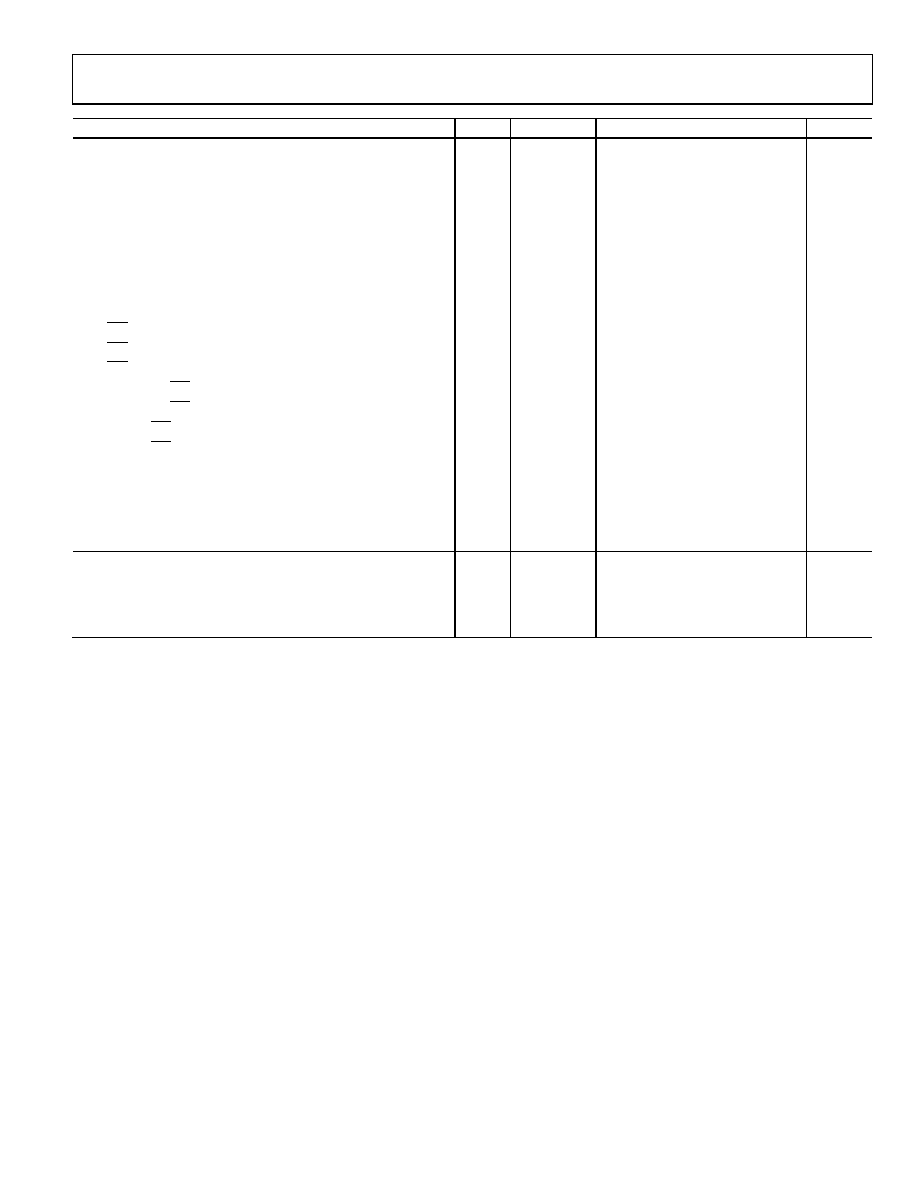
Parameter
Temp
Test Level
Min
Typ
Max
Unit
TIMING CHARACTERISTICS
Serial Control Bus
Maximum Frequency
Full
IV
10
MHz
Minimum Clock Pulse Width Low (tPWL)
Full
IV
5.5
ns
Minimum Clock Pulse Width High (tPWH)
Full
IV
15
ns
Maximum Clock Rise/Fall Time
Full
IV
1
ns
Minimum Data Setup Time (tDS)
Full
IV
7
ns
Minimum Data Hold Time (tDH)
Full
IV
0
ns
Maximum Data Valid Time (tDV)
Full
IV
20
ns
Parallel Control Bus10
WR Minimum Low Time (tWRLOW)
Full
IV
3
ns
WR Minimum High Time (tWRHIGH)
Full
IV
6
ns
WR Minimum Period (tWR)
Full
IV
9
ns
Address to WR Setup (tASU)
Full
IV
3
ns
Address to WR Hold (tAHU)
Full
IV
0
ns
Data to WR Setup (tDSU)
Full
IV
3.5
ns
Data to WR Hold (tDHU)
Full
IV
0
ns
Miscellaneous Timing Specifications
REFCLK to SYNCLK
Full
V
2.5
ns
FUD/PS[1:0] to SYNCLK Setup Time11
Full
IV
4
ns
FUD/PS[1:0] to SYNCLK Hold Time11
Full
IV
0
ns
REFCLK to SYNCLK Delay
Full
IV
2.5
3
ns
DATA LATENCY (PIPELINE DELAY)
FTW/POW to DAC Output
25°C
IV
83
SYSCLK
cycles12
DFTW to DAC Output
25°C
IV
99
SYSCLK
cycles12
1 REFCLK input is internally dc biased. AC coupling should be used.
2 Reference clock frequency is selected to ensure that the second harmonic is out of the bandwidth of interest.
3 PD inputs set at 400 MHz with divide-by-4 enabled.
4 The charge pump current is programmable in eight discrete steps; minimum value assumes current sharing.
5 For 0.75 V < VCP < CPVDD 0.75 V.
6 These differential inputs are internally dc biased. AC coupling should be used.
7 The charge pump supply voltage can range from 4.75 V to 5.25 V.
8 DAC output is differential open collector.
9 For 1 dB output compression; input power measured at 50 Ω.
10 See Figure 35 and Figure 36 for timing diagrams.
11 See Figure 34 for timing diagram.
12 SYSCLK = REFCLK/x, where x is 1 or 2, as set using CFR[6].
相關PDF資料 |
PDF描述 |
|---|---|
| AD9859YSVZ-REEL7 | IC DDS DAC 10BIT 400MSPS 48TQFP |
| AD9880KSTZ-100 | IC INTERFACE/HDMI 100MHZ 100LQFP |
| AD9882KSTZ-140 | IC INTERFACE/DVI 100MHZ 100LQFP |
| AD9883ABSTZ-RL140 | IC INTERFACE FLAT 140MHZ 80LQFP |
| AD9887AKSZ-100 | IC INTRFACE ANALOG/DVI 160-MQFP |
相關代理商/技術參數(shù) |
參數(shù)描述 |
|---|---|
| AD9858FDPCB | 制造商:AD 制造商全稱:Analog Devices 功能描述:1 GSPS Direct Digital Synthesizer |
| AD9858PCB | 制造商:AD 制造商全稱:Analog Devices 功能描述:1 GSPS Direct Digital Synthesizer |
| AD9858TLPCB | 制造商:AD 制造商全稱:Analog Devices 功能描述:1 GSPS Direct Digital Synthesizer |
| AD9858XSV | 制造商:Analog Devices 功能描述: |
| AD9859 | 制造商:AD 制造商全稱:Analog Devices 功能描述:400 MSPS, 10-Bit, 1.8 V CMOS Direct Digital Synthesizer |
發(fā)布緊急采購,3分鐘左右您將得到回復。