- 您現(xiàn)在的位置:買賣IC網(wǎng) > PDF目錄202134 > W25Q32BVZEAG (WINBOND ELECTRONICS CORP) 32M X 1 SPI BUS SERIAL EEPROM, PDSO8 PDF資料下載
參數(shù)資料
| 型號: | W25Q32BVZEAG |
| 廠商: | WINBOND ELECTRONICS CORP |
| 元件分類: | PROM |
| 英文描述: | 32M X 1 SPI BUS SERIAL EEPROM, PDSO8 |
| 封裝: | 8 X 6 MM, GREEN, WSON-8 |
| 文件頁數(shù): | 29/79頁 |
| 文件大小: | 1090K |
| 代理商: | W25Q32BVZEAG |
第1頁第2頁第3頁第4頁第5頁第6頁第7頁第8頁第9頁第10頁第11頁第12頁第13頁第14頁第15頁第16頁第17頁第18頁第19頁第20頁第21頁第22頁第23頁第24頁第25頁第26頁第27頁第28頁當前第29頁第30頁第31頁第32頁第33頁第34頁第35頁第36頁第37頁第38頁第39頁第40頁第41頁第42頁第43頁第44頁第45頁第46頁第47頁第48頁第49頁第50頁第51頁第52頁第53頁第54頁第55頁第56頁第57頁第58頁第59頁第60頁第61頁第62頁第63頁第64頁第65頁第66頁第67頁第68頁第69頁第70頁第71頁第72頁第73頁第74頁第75頁第76頁第77頁第78頁第79頁
W25Q32BV
Publication Release Date: April 01, 2011
- 35 -
Revision F
M7-0
/CS
CLK
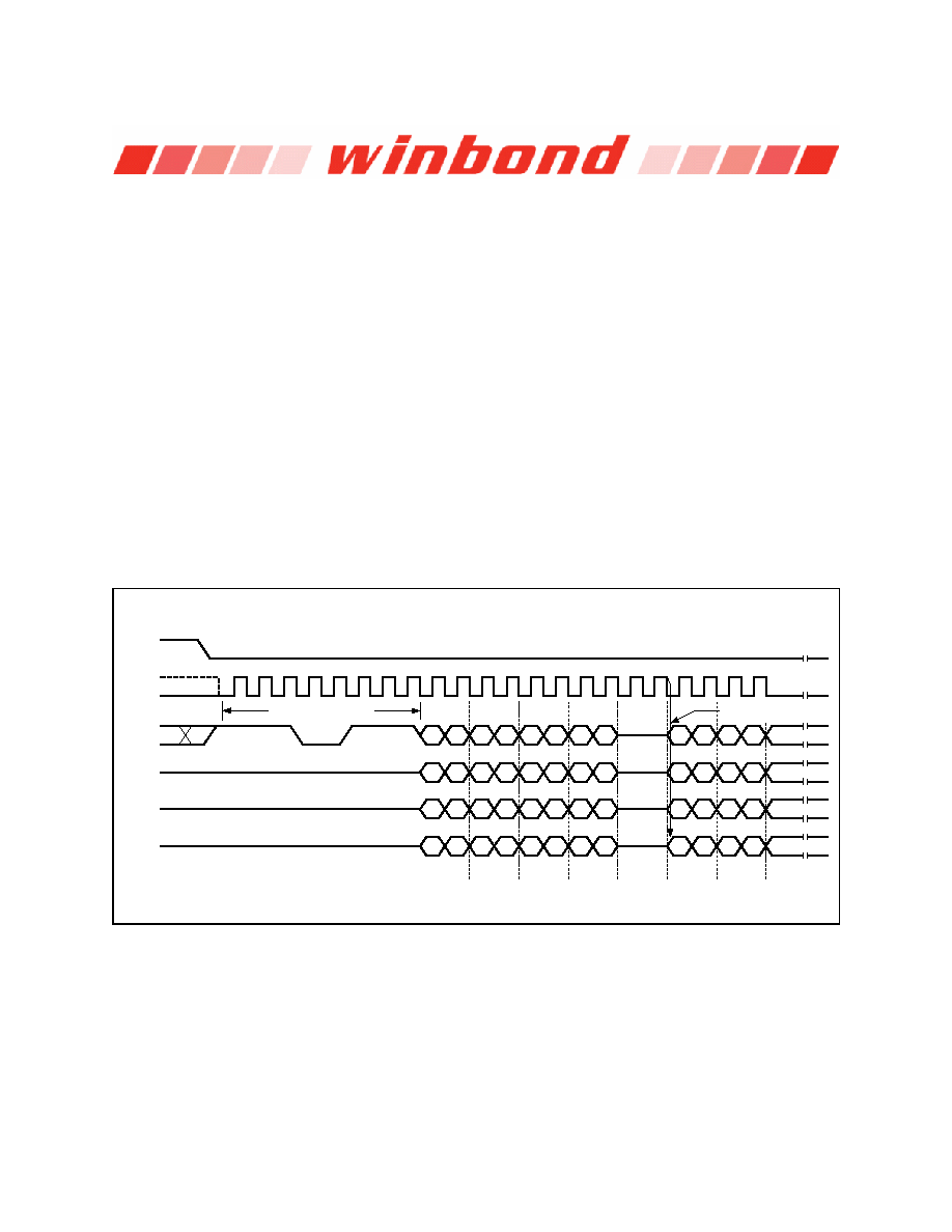
7.2.16 Word Read Quad I/O (E7h)
The Word Read Quad I/O (E7h) instruction is similar to the Fast Read Quad I/O (EBh) instruction except
that the lowest Address bit (A0) must equal 0 and only two Dummy clocks are required prior to the data
output. The Quad I/O dramatically reduces instruction overhead allowing faster random access for code
execution (XIP) directly from the Quad SPI. The Quad Enable bit (QE) of Status Register-2 must be set to
enable the Word Read Quad I/O Instruction.
Word Read Quad I/O with “Continuous Read Mode”
The Word Read Quad I/O instruction can further reduce instruction overhead through setting the
“Continuous Read Mode” bits (M7-0) after the input Address bits (A23-0), as shown in Figure 15a. The
upper nibble of the (M7-4) controls the length of the next Fast Read Quad I/O instruction through the
inclusion or exclusion of the first byte instruction code. The lower nibble bits of the (M3-0) are don’t care
(“x”). However, the IO pins should be high-impedance prior to the falling edge of the first data out clock.
If the “Continuous Read Mode” bits M5-4 = (1,0), then the next Fast Read Quad I/O instruction (after /CS
is raised and then lowered) does not require the E7h instruction code, as shown in Figure 15b. This
reduces the instruction sequence by eight clocks and allows the Read address to be immediately entered
after /CS is asserted low. If the “Continuous Read Mode” bits M5-4 do not equal to (1,0), the next
instruction (after /CS is raised and then lowered) requires the first byte instruction code, thus returning to
normal operation. A “Continuous Read Mode” Reset instruction can also be used to reset (M7-0) before
issuing normal instructions (See 7.2.20 for detail descriptions).
Figure 15a. Word Read Quad I/O Instruction Sequence (Initial instruction or previous M5-4
≠ 10)
Mode 0
Mode 3
0
1
IO
0
IO
1
IO
2
IO
3
2
3
4
5
20
16
12
8
21
17
22
18
23
19
13
9
14
10
15
11
A23-16
6
7
8
9
4
0
5
1
6
2
7
3
A15-8
A7-0
Byte 1
Byte 2
4
0
5
1
6
2
7
3
4
0
5
1
6
2
7
3
4
0
5
1
6
2
7
3
10
11
12
13
14
4
5
6
7
15
IOs switch from
Input to Output
Byte 3
16
17
18
19
20
21
Instruction (E7h)
Dummy
相關(guān)PDF資料 |
PDF描述 |
|---|---|
| W3EG6466S335AD4M | 64M X 64 DDR DRAM MODULE, 0.7 ns, DMA200 |
| W3EG7264S335AD4SG | 64M X 72 DDR DRAM MODULE, 0.7 ns, DMA200 |
| WF1M32B-120G2UI3A | 1M X 32 FLASH 3.3V PROM MODULE, 120 ns, CQFP68 |
| WF1M32B-120H1I3A | 1M X 32 FLASH 3.3V PROM MODULE, 120 ns, CPGA66 |
| WE128K32N-150G2TC | 128K X 32 EEPROM 5V MODULE, 125 ns, CQFP68 |
相關(guān)代理商/技術(shù)參數(shù) |
參數(shù)描述 |
|---|---|
| W25Q32BVZEAP | 制造商:WINBOND 制造商全稱:Winbond 功能描述:3V 32M-BIT SERIAL FLASH MEMORY WITH DUAL AND QUAD SPI |
| W25Q32BVZEIG | 制造商:Winbond Electronics Corp 功能描述:32MB SPI FLASH |
| W25Q32BVZEIP | 制造商:WINBOND 制造商全稱:Winbond 功能描述:3V 32M-BIT SERIAL FLASH MEMORY WITH DUAL AND QUAD SPI |
| W25Q32BVZPAG | 制造商:WINBOND 制造商全稱:Winbond 功能描述:3V 32M-BIT SERIAL FLASH MEMORY WITH DUAL AND QUAD SPI |
| W25Q32BVZPAP | 制造商:WINBOND 制造商全稱:Winbond 功能描述:3V 32M-BIT SERIAL FLASH MEMORY WITH DUAL AND QUAD SPI |
發(fā)布緊急采購,3分鐘左右您將得到回復。