- 您現(xiàn)在的位置:買賣IC網(wǎng) > PDF目錄383960 > TMP470R1B768PGE (Texas Instruments, Inc.) 16/32-Bit RISC Flash Microcontroller PDF資料下載
參數(shù)資料
| 型號: | TMP470R1B768PGE |
| 廠商: | Texas Instruments, Inc. |
| 英文描述: | 16/32-Bit RISC Flash Microcontroller |
| 中文描述: | 16/32位RISC閃存微控制器 |
| 文件頁數(shù): | 40/50頁 |
| 文件大小: | 393K |
| 代理商: | TMP470R1B768PGE |
第1頁第2頁第3頁第4頁第5頁第6頁第7頁第8頁第9頁第10頁第11頁第12頁第13頁第14頁第15頁第16頁第17頁第18頁第19頁第20頁第21頁第22頁第23頁第24頁第25頁第26頁第27頁第28頁第29頁第30頁第31頁第32頁第33頁第34頁第35頁第36頁第37頁第38頁第39頁當前第40頁第41頁第42頁第43頁第44頁第45頁第46頁第47頁第48頁第49頁第50頁
www.ti.com
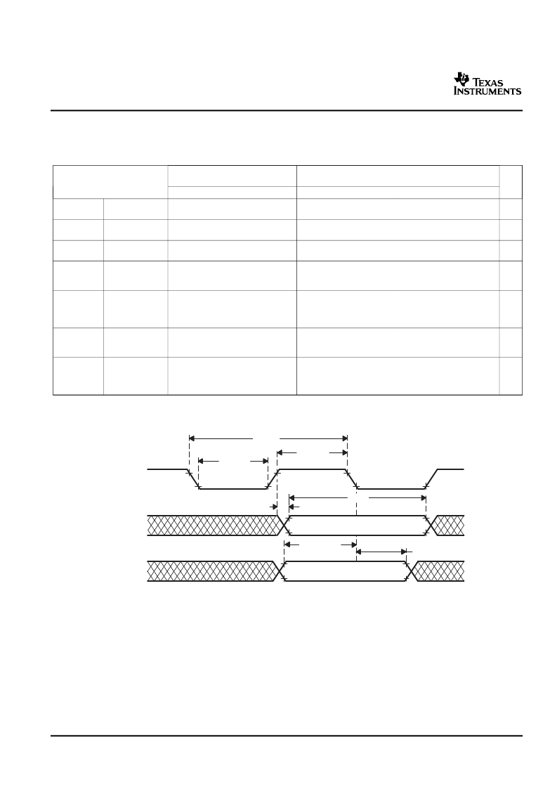
SCIn ISOSYNCHRONOUS MODE TIMINGS INTERNAL CLOCK
Timing Requirements for Internal Clock SCIn Isosynchronous Mode
(1)(2)(3)
(see
Figure 16
)
TMS470R1B768
16/32-Bit RISC Flash Microcontroller
SPNS108A–AUGUST 2005–REVISED AUGUST 2006
(BAUD + 1)
(BAUD + 1)
UNI
T
IS EVEN OR BAUD = 0
MIN
IS ODD AND BAUD
≠
0
MAX
MIN
MAX
Cycle time,
SCInCLK
Pulse duration,
SCInCLK low
Pulse duration,
SCInCLK high
Delay time,
SCInCLK high to
SCInTX valid
Valid time,
SCInTX data
after SCInCLK
low
Setup time,
SCInRX before
SCInCLK low
Valid time,
SCInRX data
after SCInCLK
low
t
c(SCC)
2t
c(ICLK)
2
24
t
c(ICLK)
3t
c(ICLK)
(2
24
-1) t
c(ICLK)
ns
t
w(SCCL)
0.5t
c(SCC)
– t
f
0.5t
c(SCC)
+ 5
0.5t
c(SCC)
+ 0.5t
c(ICLK)
– t
f
0.5t
c(SCC)
+ 0.5t
c(ICLK)
ns
t
w(SCCH)
0.5t
c(SCC)
– t
r
0.5t
c(SCC)
+ 5
0.5t
c(SCC)
– 0.5t
c(ICLK)
– t
r
0.5t
c(SCC)
– 0.5t
c(ICLK)
ns
t
d(SCCH-TXV)
10
10
ns
t
v(TX)
t
c(SCC)
– 10
t
c(SCC)
– 10
ns
t
su(RX-SCCL)
t
c(ICLK)
+ t
f
+ 20
t
c(ICLK)
+ t
f
+ 20
ns
t
v(SCCL-RX)
–t
c(ICLK)
+ t
f
+ 20
–t
c(ICLK)
+ t
f
+ 20
ns
(1)
(2)
(3)
BAUD = 24-bit concatenated value formed by the SCI[H,M,L]BAUD registers.
t
= interface clock cycle time = 1/f
For rise and fall timings, see the "Switching Characteristics for Output Timings versus Load Capacitance" table.
A.
Data transmission/reception characteristics for isosynchronous mode with internal clocking are similar to the
asynchronous mode. Data transmission occurs on the SCICLK rising edge, and data reception occurs on the
SCICLK falling edge.
Figure 16. SCIn Isosynchronous Mode Timing Diagram for Internal Clock
40
Submit Documentation Feedback
相關PDF資料 |
PDF描述 |
|---|---|
| TMP47C020 | Transient Voltage Suppressor Diodes |
| TMP47C020G | Transient Voltage Suppressor Diodes |
| TMP47C050 | Transient Voltage Suppressor Diodes |
| TMP47C050E | Transient Voltage Suppressor Diodes |
| TMP47C050G | Transient Voltage Suppressor Diodes |
相關代理商/技術參數(shù) |
參數(shù)描述 |
|---|---|
| TMP470R1F369APGEQ | 制造商:Texas Instruments 功能描述: |
| TMP470R1VF338PZQ | 制造商:Texas Instruments 功能描述:- Rail/Tube |
| TMP470R1VF478GJZQ | 制造商:Texas Instruments 功能描述: |
| TMP4720/7440P/N | 制造商:未知廠家 制造商全稱:未知廠家 功能描述: |
| TMP4720F | 制造商:未知廠家 制造商全稱:未知廠家 功能描述:4-Bit Microcontroller |
發(fā)布緊急采購,3分鐘左右您將得到回復。