- 您現(xiàn)在的位置:買賣IC網(wǎng) > PDF目錄383960 > TMP470R1B768PGE (Texas Instruments, Inc.) 16/32-Bit RISC Flash Microcontroller PDF資料下載
參數(shù)資料
| 型號: | TMP470R1B768PGE |
| 廠商: | Texas Instruments, Inc. |
| 英文描述: | 16/32-Bit RISC Flash Microcontroller |
| 中文描述: | 16/32位RISC閃存微控制器 |
| 文件頁數(shù): | 31/50頁 |
| 文件大小: | 393K |
| 代理商: | TMP470R1B768PGE |
第1頁第2頁第3頁第4頁第5頁第6頁第7頁第8頁第9頁第10頁第11頁第12頁第13頁第14頁第15頁第16頁第17頁第18頁第19頁第20頁第21頁第22頁第23頁第24頁第25頁第26頁第27頁第28頁第29頁第30頁當(dāng)前第31頁第32頁第33頁第34頁第35頁第36頁第37頁第38頁第39頁第40頁第41頁第42頁第43頁第44頁第45頁第46頁第47頁第48頁第49頁第50頁
www.ti.com
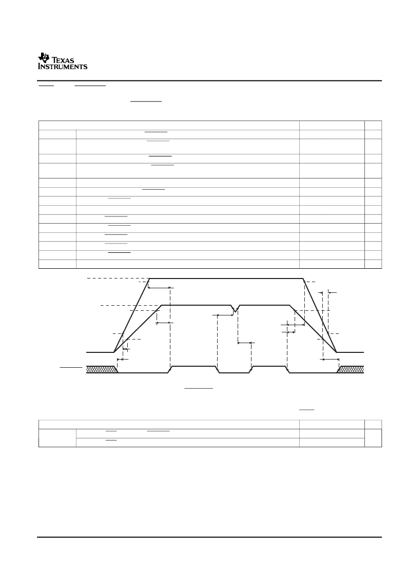
RST AND PORRST TIMINGS
Timing Requirements for PORRST
(see
Figure 8
)
Switching Characteristics over Recommended Operating Conditions for RST
(1)
TMS470R1B768
16/32-Bit RISC Flash Microcontroller
SPNS108A–AUGUST 2005–REVISED AUGUST 2006
MIN
MAX UNIT
0.6
V
CCPORL
V
CC
low supply level when PORRST must be active during power up
V
high supply level when PORRST must remain active during power up and become
active during power down
V
CCIO
low supply level when PORRST must be active during power up
V
high supply level when PORRST must remain active during power up and become
active during power down
Low-level input voltage after V
CCIO
> V
CCIOPORH
Low-level input voltage of PORRST before V
CCIO
> V
CCIOPORL
Setup time, PORRST active before V
CCIO
> V
CCIOPORL
during power up
Setup time, V
CCIO
> V
CCIOPORL
before V
CC
> V
CCPORL
Hold time, PORRST active after V
CC
> V
CCPORH
Setup time, PORRST active before V
CC
≤
V
CCPORH
during power down
Hold time, PORRST active after V
CC
V
CCIOPORH
Hold time, PORRST active after V
CC
< V
CCPORL
Setup time, PORRST active before V
CC
≤
V
CCIOPORH
during power down
Setup time, V
CC
< V
CCPORL
before V
CCIO
< V
CCIOPORL
V
V
CCPORH
1.5
V
V
CCIOPORL
1.1
V
V
CCIOPORH
2.75
V
V
IL
V
IL(PORRST)
t
su(PORRST)r
t
su(VCCIO)r
t
h(PORRST)r
t
su(PORRST)f
t
h(PORRST)rio
t
h(PORRST)d
t
su(PORRST)fio
t
su(VCCIO)f
0.2 V
CCIO
V
V
ms
ms
ms
μs
ms
ms
ns
ns
0.5
0
0
1
8
1
0
0
0
NOTE: V
CCIO
> 1.1 V before V
CC
> 0.6 V
Figure 8. PORRST Timing Diagram
PARAMETER
MIN
MAX UNIT
Valid time, RST active after PORRST inactive
Valid time, RST active (all others)
4112t
c(OSC)
8t
c(SYS)
t
v(RST)
ns
(1)
Specified values do NOT include rise/fall times. For rise and fall timings, see the "Switching Characteristics for Output Timings versus
Load Capacitance" table.
31
Submit Documentation Feedback
相關(guān)PDF資料 |
PDF描述 |
|---|---|
| TMP47C020 | Transient Voltage Suppressor Diodes |
| TMP47C020G | Transient Voltage Suppressor Diodes |
| TMP47C050 | Transient Voltage Suppressor Diodes |
| TMP47C050E | Transient Voltage Suppressor Diodes |
| TMP47C050G | Transient Voltage Suppressor Diodes |
相關(guān)代理商/技術(shù)參數(shù) |
參數(shù)描述 |
|---|---|
| TMP470R1F369APGEQ | 制造商:Texas Instruments 功能描述: |
| TMP470R1VF338PZQ | 制造商:Texas Instruments 功能描述:- Rail/Tube |
| TMP470R1VF478GJZQ | 制造商:Texas Instruments 功能描述: |
| TMP4720/7440P/N | 制造商:未知廠家 制造商全稱:未知廠家 功能描述: |
| TMP4720F | 制造商:未知廠家 制造商全稱:未知廠家 功能描述:4-Bit Microcontroller |
發(fā)布緊急采購,3分鐘左右您將得到回復(fù)。