- 您現(xiàn)在的位置:買賣IC網(wǎng) > PDF目錄98078 > SC1201UCL-266 (ADVANCED MICRO DEVICES INC) 32-BIT, 266 MHz, MICROPROCESSOR, PBGA432 PDF資料下載
參數(shù)資料
| 型號: | SC1201UCL-266 |
| 廠商: | ADVANCED MICRO DEVICES INC |
| 元件分類: | 微控制器/微處理器 |
| 英文描述: | 32-BIT, 266 MHz, MICROPROCESSOR, PBGA432 |
| 封裝: | 40 X 40 MM, 1.72 MM HEIGHT, 1.27 MM PITCH, MO-151, EBGA-432 |
| 文件頁數(shù): | 423/465頁 |
| 文件大小: | 4068K |
| 代理商: | SC1201UCL-266 |
第1頁第2頁第3頁第4頁第5頁第6頁第7頁第8頁第9頁第10頁第11頁第12頁第13頁第14頁第15頁第16頁第17頁第18頁第19頁第20頁第21頁第22頁第23頁第24頁第25頁第26頁第27頁第28頁第29頁第30頁第31頁第32頁第33頁第34頁第35頁第36頁第37頁第38頁第39頁第40頁第41頁第42頁第43頁第44頁第45頁第46頁第47頁第48頁第49頁第50頁第51頁第52頁第53頁第54頁第55頁第56頁第57頁第58頁第59頁第60頁第61頁第62頁第63頁第64頁第65頁第66頁第67頁第68頁第69頁第70頁第71頁第72頁第73頁第74頁第75頁第76頁第77頁第78頁第79頁第80頁第81頁第82頁第83頁第84頁第85頁第86頁第87頁第88頁第89頁第90頁第91頁第92頁第93頁第94頁第95頁第96頁第97頁第98頁第99頁第100頁第101頁第102頁第103頁第104頁第105頁第106頁第107頁第108頁第109頁第110頁第111頁第112頁第113頁第114頁第115頁第116頁第117頁第118頁第119頁第120頁第121頁第122頁第123頁第124頁第125頁第126頁第127頁第128頁第129頁第130頁第131頁第132頁第133頁第134頁第135頁第136頁第137頁第138頁第139頁第140頁第141頁第142頁第143頁第144頁第145頁第146頁第147頁第148頁第149頁第150頁第151頁第152頁第153頁第154頁第155頁第156頁第157頁第158頁第159頁第160頁第161頁第162頁第163頁第164頁第165頁第166頁第167頁第168頁第169頁第170頁第171頁第172頁第173頁第174頁第175頁第176頁第177頁第178頁第179頁第180頁第181頁第182頁第183頁第184頁第185頁第186頁第187頁第188頁第189頁第190頁第191頁第192頁第193頁第194頁第195頁第196頁第197頁第198頁第199頁第200頁第201頁第202頁第203頁第204頁第205頁第206頁第207頁第208頁第209頁第210頁第211頁第212頁第213頁第214頁第215頁第216頁第217頁第218頁第219頁第220頁第221頁第222頁第223頁第224頁第225頁第226頁第227頁第228頁第229頁第230頁第231頁第232頁第233頁第234頁第235頁第236頁第237頁第238頁第239頁第240頁第241頁第242頁第243頁第244頁第245頁第246頁第247頁第248頁第249頁第250頁第251頁第252頁第253頁第254頁第255頁第256頁第257頁第258頁第259頁第260頁第261頁第262頁第263頁第264頁第265頁第266頁第267頁第268頁第269頁第270頁第271頁第272頁第273頁第274頁第275頁第276頁第277頁第278頁第279頁第280頁第281頁第282頁第283頁第284頁第285頁第286頁第287頁第288頁第289頁第290頁第291頁第292頁第293頁第294頁第295頁第296頁第297頁第298頁第299頁第300頁第301頁第302頁第303頁第304頁第305頁第306頁第307頁第308頁第309頁第310頁第311頁第312頁第313頁第314頁第315頁第316頁第317頁第318頁第319頁第320頁第321頁第322頁第323頁第324頁第325頁第326頁第327頁第328頁第329頁第330頁第331頁第332頁第333頁第334頁第335頁第336頁第337頁第338頁第339頁第340頁第341頁第342頁第343頁第344頁第345頁第346頁第347頁第348頁第349頁第350頁第351頁第352頁第353頁第354頁第355頁第356頁第357頁第358頁第359頁第360頁第361頁第362頁第363頁第364頁第365頁第366頁第367頁第368頁第369頁第370頁第371頁第372頁第373頁第374頁第375頁第376頁第377頁第378頁第379頁第380頁第381頁第382頁第383頁第384頁第385頁第386頁第387頁第388頁第389頁第390頁第391頁第392頁第393頁第394頁第395頁第396頁第397頁第398頁第399頁第400頁第401頁第402頁第403頁第404頁第405頁第406頁第407頁第408頁第409頁第410頁第411頁第412頁第413頁第414頁第415頁第416頁第417頁第418頁第419頁第420頁第421頁第422頁當前第423頁第424頁第425頁第426頁第427頁第428頁第429頁第430頁第431頁第432頁第433頁第434頁第435頁第436頁第437頁第438頁第439頁第440頁第441頁第442頁第443頁第444頁第445頁第446頁第447頁第448頁第449頁第450頁第451頁第452頁第453頁第454頁第455頁第456頁第457頁第458頁第459頁第460頁第461頁第462頁第463頁第464頁第465頁
60
AMD Geode SC1200/SC1201 Processor Data Book
Signal Definitions
Revision 7.1
3.2
Strap Options
Several balls are read at power-up that set up the state of
the SC1200/SC1201 processor. These balls are typically
multiplexed with other functions that are outputs after the
power-up sequence is complete. The SC1200/SC1201 pro-
cessor must read the state of the balls at power-up and the
internal PU or PD resistors do not guarantee the correct
state will be read. Therefore, it is required that an external
PU or PD resistor with a value of 1.5 K
be placed on the
balls listed in Table 3-6. The value of the resistor is impor-
tant to ensure that the proper state is read during the
power-up sequence. If the ball is not read correctly at
power-up, the SC1200/SC1201 processor may default to a
state that causes it to function improperly, possibly result-
ing in application failure.
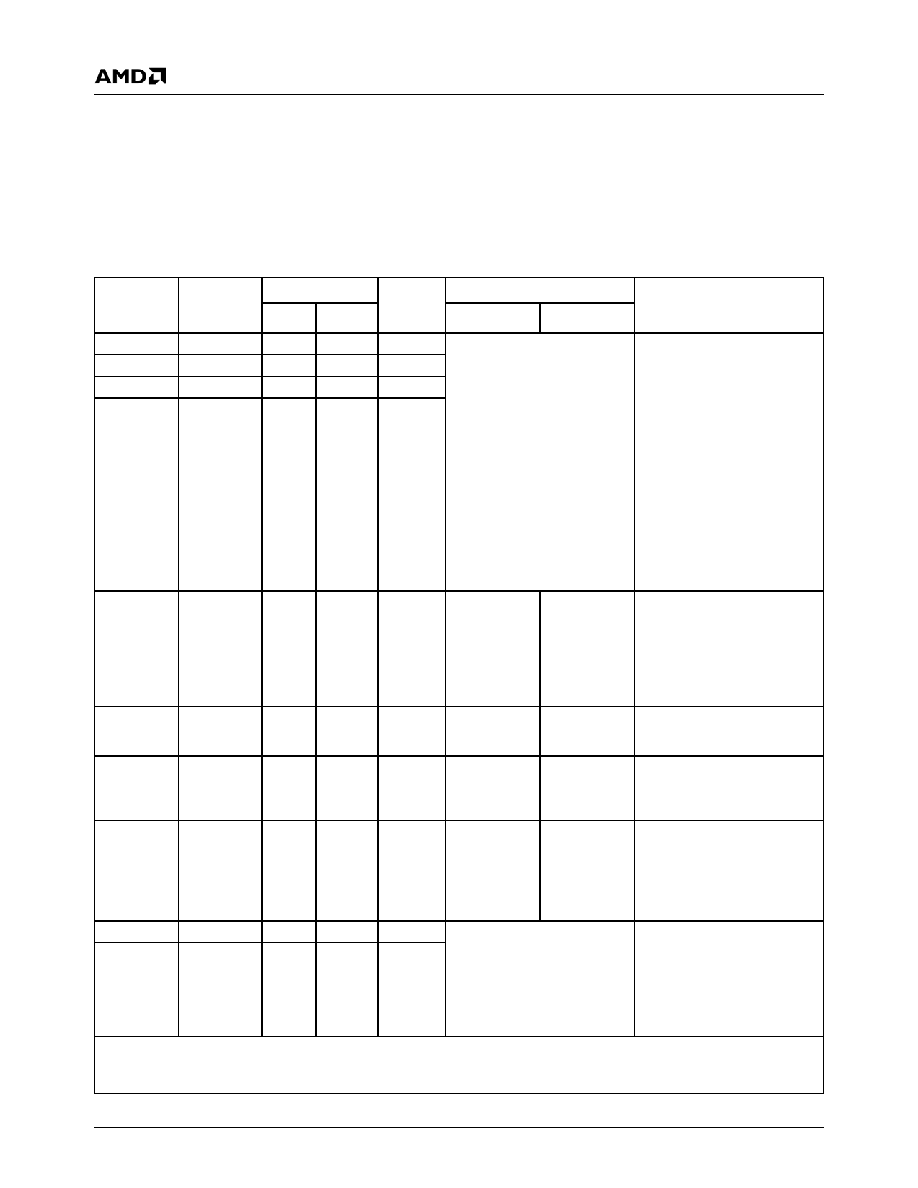
Table 3-6. Strap Options
Strap
Option
Muxed With
Ball No.
Nominal
Internal
PU or PD
External PU/PD Strap Settings
Register References
EBGA
TEPBGA
Strap = 0 (PD)
Strap = 1 (PU)
CLKSEL0
RD#
F3
B8
PD100
See Table 4-7 on page 105 for
CLKSEL strap options.
GCB+I/O Offset 1Eh[9:8] (aka
CCFC register bits [9:8]) (RO):
Value programmed at reset by
CLKSEL[1:0].
GCB+I/O Offset 10h[3:0] (aka
MCCM register bits [3:0]) (RO):
Value programmed at reset by
CLKSEL[3:0].
GCB+I/O Offset 1Eh[3:0] (aka
CCFC register bits [3:0]) (R/W,
but write not recommended):
Value programmed at reset by
CLKSEL[3:0].
Note: Values for GCB+I/O Offset
10h[3:0] and 1Eh[3:0] are not the
same.
CLKSEL1
SOUT1
B27
AF3
PD100
CLKSEL2
SOUT2
AK3
D29
PD100
CLKSEL3
SYNC
AL13
P30
PD100
BOOT16
ROMCS#
G4
C8
PD100
Enable boot
from 8-bit ROM
Enable boot
from 16-bit
ROM
GCB+I/O Offset 34h[3] (aka MCR
register bit 3) (RO): Reads back
strap setting.
GCB+I/O Offset 34h[14] (R/W):
Used to allow the ROMCS# width
to be changed under program
control.
TFT_PRSNT
SDATA_OUT
AK13
P29
PD100
TFT not muxed
onto Parallel
Port
TFT muxed
onto Parallel
Port
GCB+I/O Offset 30h[23] (aka
PMR register bit 23) (R/W):
Reads back strap setting.
LPC_ROM
PCICLK1
E4
D6
PD100
Disable boot
from ROM on
LPC bus
Enable boot
from ROM on
LPC bus
F0BAR1+I/O Offset 10h[15] (R/
W): Reads back strap setting and
allows LPC ROM to be changed
under program control.
FPCI_MON
PCICLK0
D3
A4
PD100
Disable Fast-
PCI, INTR_O,
and SMI_O
monitoring sig-
nals.
Enable Fast-
PCI, INTR_O,
and SMI_O
monitoring sig-
nals. (Useful
during debug.)
GCB+I/O Offset 34h[30] (aka
MCR register bit 30) (RO): Reads
back strap setting.
Note:
For normal operation,
strap
this
signal
low
using a 1.5 K
resistor.
DID0
GNT0#
D4
C5
PD100
Defines the system-level chip ID.
GCB+I/O Offset 34h[31,29] (aka
MCR register bits 31 and 29)
(RO): Reads back strap setting.
Note:
These signals should be
connected to a 1.5 K
PD resistor to ensure a
low level at power-up.
DID1
GNT1#
D2
C6
PD100
Note:
Accuracy of internal PU/PD resistors: 80K to 250K.
Location of the GCB (General Configuration Block) cannot be determined by software. See the AMD Geode SC1200/
SC1201 Processor Specification Update document.
相關(guān)PDF資料 |
PDF描述 |
|---|---|
| SC1201UCL-266F | 32-BIT, 266 MHz, MICROPROCESSOR, PBGA432 |
| SC12484CV-80 | PALETTE-DAC DSPL CTLR, PQCC44 |
| SC11483CV-110 | PALETTE-DAC DSPL CTLR, PQCC44 |
| SC11483CV-80 | PALETTE-DAC DSPL CTLR, PQCC44 |
| SC12482CV-80 | PALETTE-DAC DSPL CTLR, PQCC44 |
相關(guān)代理商/技術(shù)參數(shù) |
參數(shù)描述 |
|---|---|
| SC1201UCL-266 D3 | 制造商:Advanced Micro Devices 功能描述: |
| SC1201UFH-266 | 制造商:Rochester Electronics LLC 功能描述:- Bulk 制造商:Advanced Micro Devices 功能描述: 制造商:AMD 功能描述: |
| SC1201UFH-266B | 制造商:Rochester Electronics LLC 功能描述:- Bulk |
| SC1201UFH-266F | 制造商:Rochester Electronics LLC 功能描述:- Bulk |
| SC1201UFH-266FR | 制造商:Rochester Electronics LLC 功能描述:- Bulk |
發(fā)布緊急采購,3分鐘左右您將得到回復(fù)。