- 您現(xiàn)在的位置:買賣IC網(wǎng) > PDF目錄382380 > PCD5003A (NXP Semiconductors N.V.) Enhanced Pager Decoder for POCSAG PDF資料下載
參數(shù)資料
| 型號: | PCD5003A |
| 廠商: | NXP Semiconductors N.V. |
| 英文描述: | Enhanced Pager Decoder for POCSAG |
| 中文描述: | 增強傳呼機POCSAG碼解碼器 |
| 文件頁數(shù): | 17/44頁 |
| 文件大小: | 233K |
| 代理商: | PCD5003A |
第1頁第2頁第3頁第4頁第5頁第6頁第7頁第8頁第9頁第10頁第11頁第12頁第13頁第14頁第15頁第16頁當(dāng)前第17頁第18頁第19頁第20頁第21頁第22頁第23頁第24頁第25頁第26頁第27頁第28頁第29頁第30頁第31頁第32頁第33頁第34頁第35頁第36頁第37頁第38頁第39頁第40頁第41頁第42頁第43頁第44頁

1999 Jan 08
17
Philips Semiconductors
Product specification
Enhanced Pager Decoder for POCSAG
PCD5003A
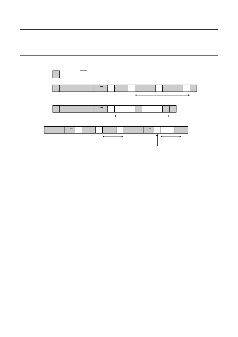
Fig.8 Message types.
(a) Master writes to slave.
(b) Master reads from slave.
(c) Combined format (shown: write plus read).
handbook, full pagewidth
n bytes with acknowledge
FROM
MASTER
FROM
SLAVE
A
A
S
SLAVE ADDRESS
R/W
DATA
A
DATA
A
P
S = START condition
P = STOP condition
A = Acknowledge
N = Not acknowledge
n bytes with acknowledge
A
S
SLAVE ADDRESS
R/W
DATA
DATA
P
A
(a)
(b)
(c)
R/W
DATA
SL. ADR.
SL. ADR.
R/W
DATA
0 (write)
0 (write)
1 (read)
1 (read)
index
address
index
address
n bytes with
acknowledge
n bytes with
acknowledge
change of direction
N
A
A
A
INDEX
INDEX
A
S
S
N
P
MLC250
7.25
Decoder I
2
C-bus access
All internal access to the PCD5003A takes place via the
I
2
C-bus interface. For this purpose the internal registers,
SRAM and EEPROM have been memory mapped and are
accessed via an
index register
. Table 13 shows the index
addresses of all internal blocks.
Registers are addressed directly, while RAM and
EEPROM are addressed indirectly via address pointers
and I/O registers.
Remark
: The EEPROM memory map is non-contiguous
and organized as a matrix. The EEPROM address pointer
contains both row and column indicators.
Data written to read-only bits will be ignored. Values read
from write-only bits are undefined and must be ignored.
Each I
2
C-bus write message to the PCD5003A must start
with its slave address, followed by the index address of the
memory element to be accessed. An I
2
C-bus read
message uses the last written index address as a data
source. The different I
2
C-bus message types are shown in
Fig.8.
As a slave the PCD5003A cannot initiate bus transfers by
itself. To prevent an external controller from having to
monitor the operating status of the decoder, all important
events generate an external interrupt on output INT.
相關(guān)PDF資料 |
PDF描述 |
|---|---|
| PCD5003AH | Enhanced Pager Decoder for POCSAG |
| PCD5003 | Advanced POCSAG Paging Decoder |
| PCD5003H | Advanced POCSAG Paging Decoder |
| PCD5008 | FLEX Pager Decoder |
| PCD5008H | FLEX Pager Decoder |
相關(guān)代理商/技術(shù)參數(shù) |
參數(shù)描述 |
|---|---|
| PCD5003AH | 制造商:PHILIPS 制造商全稱:NXP Semiconductors 功能描述:Enhanced Pager Decoder for POCSAG |
| PCD5003H | 制造商:PHILIPS 制造商全稱:NXP Semiconductors 功能描述:Advanced POCSAG Paging Decoder |
| PCD5003HB-T | 制造商:未知廠家 制造商全稱:未知廠家 功能描述:Telecommunication Decoder |
| PCD5003U/10 | 制造商:PHILIPS 制造商全稱:NXP Semiconductors 功能描述:Advanced POCSAG Paging Decoder |
| PCD5008 | 制造商:PHILIPS 制造商全稱:NXP Semiconductors 功能描述:FLEX Pager Decoder |
發(fā)布緊急采購,3分鐘左右您將得到回復(fù)。