- 您現(xiàn)在的位置:買賣IC網(wǎng) > PDF目錄359155 > MCZ33989EG (飛思卡爾半導(dǎo)體(中國(guó))有限公司) System Basis Chip with High-Speed CAN Transceiver PDF資料下載
參數(shù)資料
| 型號(hào): | MCZ33989EG |
| 廠商: | 飛思卡爾半導(dǎo)體(中國(guó))有限公司 |
| 元件分類: | CAN |
| 英文描述: | System Basis Chip with High-Speed CAN Transceiver |
| 中文描述: | 系統(tǒng)基礎(chǔ)芯片高高速CAN收發(fā)器 |
| 文件頁(yè)數(shù): | 3/66頁(yè) |
| 文件大小: | 1181K |
| 代理商: | MCZ33989EG |
第1頁(yè)第2頁(yè)當(dāng)前第3頁(yè)第4頁(yè)第5頁(yè)第6頁(yè)第7頁(yè)第8頁(yè)第9頁(yè)第10頁(yè)第11頁(yè)第12頁(yè)第13頁(yè)第14頁(yè)第15頁(yè)第16頁(yè)第17頁(yè)第18頁(yè)第19頁(yè)第20頁(yè)第21頁(yè)第22頁(yè)第23頁(yè)第24頁(yè)第25頁(yè)第26頁(yè)第27頁(yè)第28頁(yè)第29頁(yè)第30頁(yè)第31頁(yè)第32頁(yè)第33頁(yè)第34頁(yè)第35頁(yè)第36頁(yè)第37頁(yè)第38頁(yè)第39頁(yè)第40頁(yè)第41頁(yè)第42頁(yè)第43頁(yè)第44頁(yè)第45頁(yè)第46頁(yè)第47頁(yè)第48頁(yè)第49頁(yè)第50頁(yè)第51頁(yè)第52頁(yè)第53頁(yè)第54頁(yè)第55頁(yè)第56頁(yè)第57頁(yè)第58頁(yè)第59頁(yè)第60頁(yè)第61頁(yè)第62頁(yè)第63頁(yè)第64頁(yè)第65頁(yè)第66頁(yè)
Analog Integrated Circuit Device Data
Freescale Semiconductor
3
33989
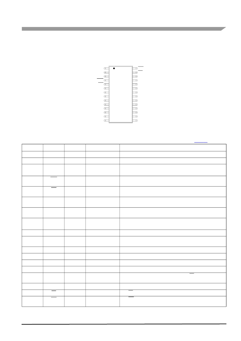
PIN CONNECTIONS
PIN CONNECTIONS
Figure 3. 33989 Pin Connections
Table 1. 33989 Pin Definitions
A functional description of each pin can be found in the Functional Pin Description section beginning on
page 18
.
Pin Number
Pin Name
Pin Function
Formal Name
Definition
1
RX
Output
Receive Data
CAN bus receive data output pin.
2
TX
Input
Transmit Data
CAN bus transmit data input pin.
3
VDD1
Power
Output
Voltage Digital Drain
One
5.0 V regulator output pin. Supply pin for the MCU.
4
RST
Output
Reset
This is the device reset output pin whose main function is to reset the
MCU. This pin has an internal pullup current source to VDD.
5
INT
Output
Interrupt
This output is asserted LOW when an enabled interrupt condition occurs.
The output is a push-pull structure.
6–9
20–23
GND
Ground
Ground
These device ground pins are internally connected to the package lead
frame to provide a 33989-to-PCB thermal path.
10
V2
Input
Voltage Source Two
Sense input for the V2 regulator using an external series pass transistor.
V2 is also the internal supply for the CAN transceiver.
11
V2CTRL
Power
Output
Voltage Control
Output drive source for the V2 regulator connected to the external series
pass transistor.
12
VSUP
Power
Voltage Supply
Supply input pin for the 33989.
13
HS1
Output
High Side One
Output of the internal high-side switch. The output current is internally
limited to 150 mA.
14–17
L0:L3
Input
Level 0: 3
Inputs from external switches or from logic circuitry.
22
CANH
Output
CAN High
CAN high output pin.
23
CANL
Output
CAN Low
CAN low output pin.
24
SCLK
Input
System Clock
Clock input pin for the Serial Peripheral Interface (SPI).
25
MISO
Output
Master In/Slave Out
SPI data sent to the MCU by the 33989. When CS is HIGH, the pin is in
the high-impedance state.
26
MOSI
Input
Master Out/Slave In
SPI data received by the 33989.
27
CS
Input
Chip Select
The CS input pin is used with the SPI bus to select the 33989.
28
WD
Output
Watch Dog
The WD output pin is asserted LOW if the software watchdog is not
correctly triggered.
WD
CS
MOSI
MISO
SCLK
GND
GND
GND
GND
CANL
CANH
L3
L2
L1
RX
TX
RST
INT
GND
GND
GND
GND
V2
V2CTRL
VSUP
HS1
L0
VDD1
4
5
6
7
8
9
10
11
12
13
14
2
3
28
27
26
25
24
23
22
21
20
19
18
17
16
15
1
相關(guān)PDF資料 |
PDF描述 |
|---|---|
| MCZ33990EF | Enhanced Class B Serial Transceiver |
| MCZ33991EG | Gauge Driver Integrated Circuit |
| MCZ33993EW | Multiple Switch Detection Interface |
| MCZ33996EK | 16-Output Switch with SPI Control |
| MCZ34652EF | 2.0 A Negative Voltage Hot Swap Controller with Enhanced Programmability |
相關(guān)代理商/技術(shù)參數(shù) |
參數(shù)描述 |
|---|---|
| MCZ33989EG | 制造商:Freescale Semiconductor 功能描述:IC SYSTEM BASIS W/CAN TRANCEIVER |
| MCZ33989EGR2 | 功能描述:網(wǎng)絡(luò)控制器與處理器 IC SBC-HS RoHS:否 制造商:Micrel 產(chǎn)品:Controller Area Network (CAN) 收發(fā)器數(shù)量: 數(shù)據(jù)速率: 電源電流(最大值):595 mA 最大工作溫度:+ 85 C 安裝風(fēng)格:SMD/SMT 封裝 / 箱體:PBGA-400 封裝:Tray |
| MCZ33990EF | 功能描述:網(wǎng)絡(luò)控制器與處理器 IC CLASS B SERIAL TRANS. RoHS:否 制造商:Micrel 產(chǎn)品:Controller Area Network (CAN) 收發(fā)器數(shù)量: 數(shù)據(jù)速率: 電源電流(最大值):595 mA 最大工作溫度:+ 85 C 安裝風(fēng)格:SMD/SMT 封裝 / 箱體:PBGA-400 封裝:Tray |
| MCZ33990EF | 制造商:Freescale Semiconductor 功能描述:TRANCEIVER J-1850 CLASS B 8SOIC |
| MCZ33990EF/R2 | 制造商:FREESCALE 制造商全稱:Freescale Semiconductor, Inc 功能描述:Enhanced Class B Serial Transceiver |
發(fā)布緊急采購(gòu),3分鐘左右您將得到回復(fù)。