- 您現(xiàn)在的位置:買賣IC網(wǎng) > PDF目錄359155 > MCZ33989EG (飛思卡爾半導(dǎo)體(中國)有限公司) System Basis Chip with High-Speed CAN Transceiver PDF資料下載
參數(shù)資料
| 型號: | MCZ33989EG |
| 廠商: | 飛思卡爾半導(dǎo)體(中國)有限公司 |
| 元件分類: | CAN |
| 英文描述: | System Basis Chip with High-Speed CAN Transceiver |
| 中文描述: | 系統(tǒng)基礎(chǔ)芯片高高速CAN收發(fā)器 |
| 文件頁數(shù): | 17/66頁 |
| 文件大?。?/td> | 1181K |
| 代理商: | MCZ33989EG |
第1頁第2頁第3頁第4頁第5頁第6頁第7頁第8頁第9頁第10頁第11頁第12頁第13頁第14頁第15頁第16頁當(dāng)前第17頁第18頁第19頁第20頁第21頁第22頁第23頁第24頁第25頁第26頁第27頁第28頁第29頁第30頁第31頁第32頁第33頁第34頁第35頁第36頁第37頁第38頁第39頁第40頁第41頁第42頁第43頁第44頁第45頁第46頁第47頁第48頁第49頁第50頁第51頁第52頁第53頁第54頁第55頁第56頁第57頁第58頁第59頁第60頁第61頁第62頁第63頁第64頁第65頁第66頁
Analog Integrated Circuit Device Data
Freescale Semiconductor
17
33989
ELECTRICAL CHARACTERISTICS
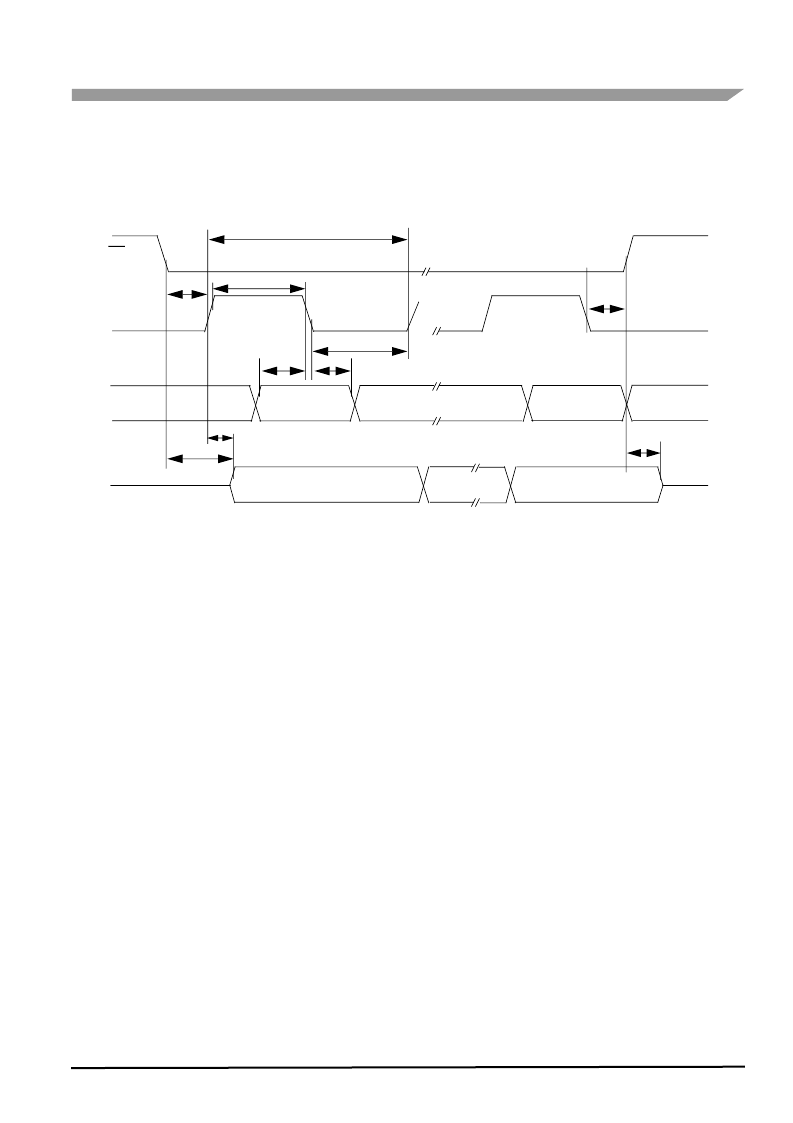
TIMING DIAGRAMS
TIMING DIAGRAMS
Figure 8. SPI Timing Characteristics
Di 0
Do 0
Undefined
Don’t Care
Di 8
Don’t Care
t
LEAD
t
SIH
t
SISU
t
LAG
t
PCLK
t
WCLKH
t
WCLKL
t
VALID
Do 8
t
SODIS
CS
SCLK
MOSI
MISO
t
SOEN
Incoming data at MOSI pin is sampled by the SBC at SCLK falling edge.
Outgoing data at MISO pin is set by the SBC at SCLK rising edge (after t
VALID
delay time).
Notes:
發(fā)布緊急采購,3分鐘左右您將得到回復(fù)。