- 您現(xiàn)在的位置:買賣IC網(wǎng) > PDF目錄180051 > M-ORSO82G52BM680-DB (LATTICE SEMICONDUCTOR CORP) FPGA, 1296 CLBS, 333000 GATES, PBGA680 PDF資料下載
參數(shù)資料
| 型號(hào): | M-ORSO82G52BM680-DB |
| 廠商: | LATTICE SEMICONDUCTOR CORP |
| 元件分類: | FPGA |
| 英文描述: | FPGA, 1296 CLBS, 333000 GATES, PBGA680 |
| 封裝: | PLASTIC, FBGA-680 |
| 文件頁(yè)數(shù): | 115/123頁(yè) |
| 文件大小: | 2207K |
| 代理商: | M-ORSO82G52BM680-DB |
第1頁(yè)第2頁(yè)第3頁(yè)第4頁(yè)第5頁(yè)第6頁(yè)第7頁(yè)第8頁(yè)第9頁(yè)第10頁(yè)第11頁(yè)第12頁(yè)第13頁(yè)第14頁(yè)第15頁(yè)第16頁(yè)第17頁(yè)第18頁(yè)第19頁(yè)第20頁(yè)第21頁(yè)第22頁(yè)第23頁(yè)第24頁(yè)第25頁(yè)第26頁(yè)第27頁(yè)第28頁(yè)第29頁(yè)第30頁(yè)第31頁(yè)第32頁(yè)第33頁(yè)第34頁(yè)第35頁(yè)第36頁(yè)第37頁(yè)第38頁(yè)第39頁(yè)第40頁(yè)第41頁(yè)第42頁(yè)第43頁(yè)第44頁(yè)第45頁(yè)第46頁(yè)第47頁(yè)第48頁(yè)第49頁(yè)第50頁(yè)第51頁(yè)第52頁(yè)第53頁(yè)第54頁(yè)第55頁(yè)第56頁(yè)第57頁(yè)第58頁(yè)第59頁(yè)第60頁(yè)第61頁(yè)第62頁(yè)第63頁(yè)第64頁(yè)第65頁(yè)第66頁(yè)第67頁(yè)第68頁(yè)第69頁(yè)第70頁(yè)第71頁(yè)第72頁(yè)第73頁(yè)第74頁(yè)第75頁(yè)第76頁(yè)第77頁(yè)第78頁(yè)第79頁(yè)第80頁(yè)第81頁(yè)第82頁(yè)第83頁(yè)第84頁(yè)第85頁(yè)第86頁(yè)第87頁(yè)第88頁(yè)第89頁(yè)第90頁(yè)第91頁(yè)第92頁(yè)第93頁(yè)第94頁(yè)第95頁(yè)第96頁(yè)第97頁(yè)第98頁(yè)第99頁(yè)第100頁(yè)第101頁(yè)第102頁(yè)第103頁(yè)第104頁(yè)第105頁(yè)第106頁(yè)第107頁(yè)第108頁(yè)第109頁(yè)第110頁(yè)第111頁(yè)第112頁(yè)第113頁(yè)第114頁(yè)當(dāng)前第115頁(yè)第116頁(yè)第117頁(yè)第118頁(yè)第119頁(yè)第120頁(yè)第121頁(yè)第122頁(yè)第123頁(yè)
Lattice Semiconductor
ORCA ORSO82G5 Data Sheet
91
Pin Information
Pin Descriptions
This section describes the pins found on the Series 4 FPGAs. Any pin not described in this table is a user-program-
mable I/O. During conguration, the user-programmable I/Os are 3-stated with an internal pull-up resistor. If any pin
is not used (or not bonded to a package pin), it is also 3-stated with an internal pull-up resistor after conguration.
The pin descriptions in Table 32. and throughout this data sheet show active-low signals with an overscore. The
package pinout tables that follow, show this as a signal ending with _N. For example LDC and LDC_N are equiva-
lent.
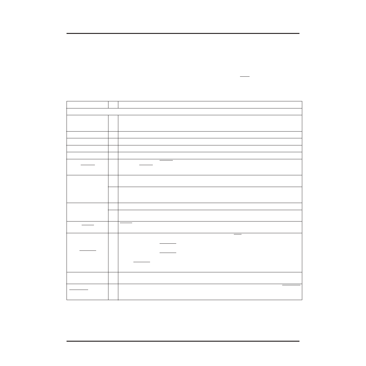
Table 32. Pin Descriptions
Symbol
I/O
Description
Dedicated Pins
VDD33
—
3.3 V positive power supply. This power supply is used for 3.3 V conguration RAMs and internal
PLLs. When using PLLs, this power supply should be well isolated from all other power supplies on
the board for proper operation.
VDD
15
—
1.5 V positive power supply for internal logic.
VDDIO
—
Positive power supply used by I/O banks.
VSS
—
Ground.
PTEMP
I
Temperature sensing diode pin. Dedicated input.
RESET
I
During conguration, RESET forces the restart of conguration and a pull-up is enabled. After con-
guration, RESET can be used as a general FPGA input or as a direct input, which causes all PLC
latches/FFs to be asynchronously set/reset.
CCLK
O
In the master and asynchronous peripheral modes, CCLK is an output which strobes conguration
data in.
I
In the slave or readback after conguration, CCLK is input synchronous with the data on DIN or
D[7:0]. CCLK is an output for daisy-chain operation when the lead device is in master, peripheral, or
system bus modes.
DONE
I
As an input, a low level on DONE delays FPGA start-up after conguration.*
O
As an active-high, open-drain output, a high level on this signal indicates that conguration is com-
plete. DONE has an optional pull-up resistor.
PRGM
I
PRGM
is an active-low input that forces the restart of conguration and resets the boundary-scan
circuitry. This pin always has an active pull-up.
RD_CFG
I
This pin must be held high during device initialization until the INIT pin goes high. This pin always
has an active pull-up.
During conguration, RD_CFG is an active-low input that activates the TS_ALL function and 3-
states all of the I/O.
After conguration, RD_CFG can be selected (via a bit stream option) to activate the TS_ALL
function as described above, or, if readback is enabled via a bit stream option, a high-to-low transi-
tion on RD_CFG will initiate readback of the conguration data, including PFU output states, start-
ing with frame address 0.
RD_DATA/TDO
O
RD_DATA/TDO is a dual-function pin. If used for readback, RD_DATA provides conguration data
out. If used in boundary-scan, TDO is test data out.
CFG_IRQ/MPI_IRQ
O
During JTAG, slave, master, and asynchronous peripheral conguration assertion on this CFG_IRQ
(active-low) indicates an error or errors for block RAM or FPSC initialization.
MPI active-low inter-
rupt request output, when the MPI is used.
* The FPGA States of Operation section contains more information on how to control these signals during start-up. The timing of DONE release
is controlled by one set of bit stream options, and the timing of the simultaneous release of all other conguration pins (and the activation of all
user I/Os) is controlled by a second set of options.
相關(guān)PDF資料 |
PDF描述 |
|---|---|
| M-ORT82G51BM680-DB | FPGA, 1296 CLBS, 333000 GATES, PBGA680 |
| M-ORT82G52BM680-DB | FPGA, 1296 CLBS, 333000 GATES, PBGA680 |
| M.PI-1R1D12 | 1 ELEMENT, 1.1 uH, GENERAL PURPOSE INDUCTOR, SMD |
| M01-014-1452PA | 14 CONTACT(S), MALE, RIGHT ANGLE TELECOM AND DATACOM CONNECTOR, SOLDER |
| M01-016-1443PA | 16 CONTACT(S), MALE, RIGHT ANGLE TELECOM AND DATACOM CONNECTOR, SOLDER |
相關(guān)代理商/技術(shù)參數(shù) |
參數(shù)描述 |
|---|---|
| MORTAR-44LB | 制造商:3M Electronic Products Division 功能描述:3M(TM) FIRE BARRIER MORTAR, 44 98040056073 制造商:3M Electronic Products Division 功能描述:Fire Barrier 44 lb Bag |
| MO-RX3930 | 制造商:未知廠家 制造商全稱:未知廠家 功能描述:FSK RECEIVER MODULE |
| MO-RX3930-FS | 制造商:未知廠家 制造商全稱:未知廠家 功能描述:FSK RECEIVER MODULE |
| MO-RX3930-FS315M | 制造商:未知廠家 制造商全稱:未知廠家 功能描述:FSK RECEIVER MODULE |
| MO-RX3930-FS434M | 制造商:未知廠家 制造商全稱:未知廠家 功能描述:FSK RECEIVER MODULE |
發(fā)布緊急采購(gòu),3分鐘左右您將得到回復(fù)。