- 您現(xiàn)在的位置:買賣IC網(wǎng) > PDF目錄385396 > HSP50415EVAL1 (Intersil Corporation) HSP50415EVAL1 Evaluation Kit PDF資料下載
參數(shù)資料
| 型號(hào): | HSP50415EVAL1 |
| 廠商: | Intersil Corporation |
| 英文描述: | HSP50415EVAL1 Evaluation Kit |
| 中文描述: | HSP50415EVAL1評(píng)估板 |
| 文件頁(yè)數(shù): | 14/29頁(yè) |
| 文件大?。?/td> | 229K |
| 代理商: | HSP50415EVAL1 |
第1頁(yè)第2頁(yè)第3頁(yè)第4頁(yè)第5頁(yè)第6頁(yè)第7頁(yè)第8頁(yè)第9頁(yè)第10頁(yè)第11頁(yè)第12頁(yè)第13頁(yè)當(dāng)前第14頁(yè)第15頁(yè)第16頁(yè)第17頁(yè)第18頁(yè)第19頁(yè)第20頁(yè)第21頁(yè)第22頁(yè)第23頁(yè)第24頁(yè)第25頁(yè)第26頁(yè)第27頁(yè)第28頁(yè)第29頁(yè)
4-14
I/Q Gain Imbalance Correction Stage
Following the X/SIN(X) filter pair is a gain stage where I and
Q are scaled independently. The programmable gain
consists of a 10-bit scale factor and a 10-bit DC offset. The
equation for the gain is as follows:
dataOut<15:0> = (dataIn<15:0> * (1.0 +/-
0.00SSSSSSSSSS)) +/- 0.00DDDDDDDDDD
Where SSSSSSSSSS denotes the 10-bit scale factor and
DDDDDDDDDD is the 10-bit DC offset value. The scale
factor may be optionally added or subtracted from 1.0 and
the DC offset may optionally be added or subtracted to the
result of the scale operation.
For a gain of 1.0 through this stage, program the scale factor
to 0x000 and the DC offset to 0x000 for both the I and Q
values. The output is rounded to either 14-bits or 12-bits.
The rounding options are programmable as shown in
Table 4.
If saturation does occur, the output is symmetrically limited.
Digital to Analog (D/A) Converters
The HSP50415 outputs using dual 12-bit, 150MSPS, high
speed, low power, D/A converters. The converter provides
20mA of full scale output current and includes edge-
triggered CMOS input data latches. Low glitch energy and
excellent frequency domain performance is achieved by the
DACs segmented current source architecture.
Voltage Reference
The internal voltage reference of the device has a nominal
value of + 1.2V with a
±
10ppm/
o
C drift coefficient over the full
temperature range of the converter. It is recommended that a
0.1
μ
F capacitor be placed as close as possible to the REFIO
pin, connected to the analog ground. The REFLO pin selects
the reference. The internal reference can be selected if
REFLO is tied low (ground). If an external reference is
desired, then REFLO should be tied high (the analog supply
voltage) and the external reference driven into REFIO. The full
scale output current of the converter is a function of the
voltage reference used and the value of R
SET
. I
OUT
should
be within the 2mA to 20mA range, though operation below
2mA is possible, with performance degradation.
V
FSADJ
and V
REFIO
will be equivalent except for a small
offset voltage. If the internal reference is used, V
FSADJ
will
equal approximately 1.2V on the FSADJ. If an external
reference is used, V
FSADJ
will equal the external reference.
The calculation for I
OUT
(Full Scale) is:
I
OUT
(Full Scale) = (V
FSADJ
/R
SET
) X 32.
If the full scale output current is set to 20mA by using the
internal voltage reference (1.2V) and a 1.91k
R
SET
resistor, then the input coding to output current is shown in
Table 5.
Outputs
The 5 MSBs for each DAC on the HSP50415 drive a
thermometer decoder
,
which is a digital decoder that has a
5-bit binary coded input word with 2
5
-1 (or 31) output bits,
where the number of output bits that are active correlate
directly to the input binary word. The HSP50415 uses a
thermometer decoder to significantly minimize the output
glitch energy for each DAC. I/QOUTA and I/QOUTB are
complementary current outputs. The sum of the two currents
is always equal to the full scale output current minus one
LSB. If single ended use is desired, a load resistor can be
used to convert the output current to a voltage. It is
recommended that the unused output be either grounded or
equally terminated. The voltage developed at the output
must not violate the output voltage compliance range of -
0.3V to 1.25V. R
LOAD
(the impedance loading each current
output) should be chosen so that the desired output voltage
is produced in conjunction with the output full scale current.
If a known line impedance is to be driven, then the output
load resistor should be chosen to match this impedance.
The output voltage equation is:
V
OUT
= I
OUT
X R
LOAD
.
TABLE 4. IQ GAIN CORRECTION STAGE ROUNDING OPTIONS
RNDBITS<1:0>
ROUND SELECTION
00
No rounding performed, data is truncated
01
Round to 14-bits
10
Round to 12-bits
11
Round in both positions
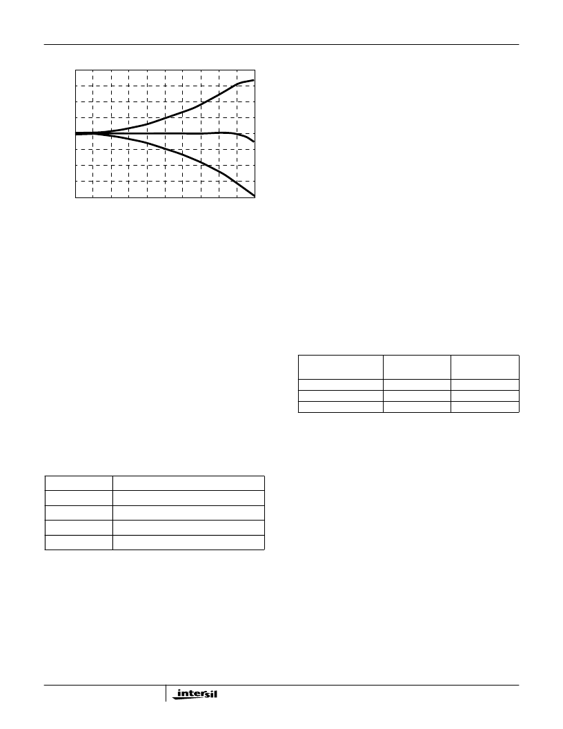
FIGURE 18. X/SIN(X) FILTER RESPONSE
4
3
2
1
0
-1
-2
-3
-4
0
0.05
0.1
0.15
0.2
0.25
0.3
0.35
0.4
0.45
0.5
ISF
SINC
NORMALIZED FREQUENCY
L
TABLE 5. INPUT CODING vs OUTPUT CURRENT
INPUT CODE <D11-
D0>
I/QOUTA (mA)
I/QOUTB (mA)
11 11111 11111
10 00000 00000
00 00000 00000
20
10
0
0
10
20
HSP50415
相關(guān)PDF資料 |
PDF描述 |
|---|---|
| HSP9501 | Programmable Data Buffer(可編程數(shù)據(jù)緩沖器) |
| HSP9520 | Multilevel Pipeline Registers |
| HSP9520CP | Multilevel Pipeline Registers |
| HSP9520CS | Multilevel Pipeline Registers |
| HSP9521 | Multilevel Pipeline Registers |
相關(guān)代理商/技術(shù)參數(shù) |
參數(shù)描述 |
|---|---|
| HSP50415VI | 功能描述:調(diào)節(jié)器/解調(diào)器 100MQFP, -40+85C,PROGRAMABLE MODULATOR RoHS:否 制造商:Texas Instruments 封裝 / 箱體:PVQFN-N24 封裝:Reel |
| HSP50415VIZ | 功能描述:調(diào)節(jié)器/解調(diào)器 W/ANL 100MQFP-40+85C PROGRAMABLE MODLTR RoHS:否 制造商:Texas Instruments 封裝 / 箱體:PVQFN-N24 封裝:Reel |
| HSP50A | 制造商:JLWORLD 制造商全稱:JLWORLD 功能描述:SPEAKER SOUND GENERATORS |
| HSP50B | 制造商:JLWORLD 制造商全稱:JLWORLD 功能描述:SPEAKER SOUND GENERATORS |
| HSP50SA8 | 制造商:RDI 功能描述:SPEAKER 2 ROUND 8 OHMS CLEAR FACE |
發(fā)布緊急采購(gòu),3分鐘左右您將得到回復(fù)。