- 您現(xiàn)在的位置:買賣IC網(wǎng) > PDF目錄374033 > ADSP-21262SKSTZ200 (ANALOG DEVICES INC) SHARC Processor PDF資料下載
參數(shù)資料
| 型號(hào): | ADSP-21262SKSTZ200 |
| 廠商: | ANALOG DEVICES INC |
| 元件分類: | 數(shù)字信號(hào)處理 |
| 英文描述: | SHARC Processor |
| 中文描述: | 16-BIT, 66.67 MHz, OTHER DSP, PQFP144 |
| 封裝: | LEAD FREE, MS-026BFB, LQFP-144 |
| 文件頁(yè)數(shù): | 18/44頁(yè) |
| 文件大小: | 1295K |
| 代理商: | ADSP-21262SKSTZ200 |
第1頁(yè)第2頁(yè)第3頁(yè)第4頁(yè)第5頁(yè)第6頁(yè)第7頁(yè)第8頁(yè)第9頁(yè)第10頁(yè)第11頁(yè)第12頁(yè)第13頁(yè)第14頁(yè)第15頁(yè)第16頁(yè)第17頁(yè)當(dāng)前第18頁(yè)第19頁(yè)第20頁(yè)第21頁(yè)第22頁(yè)第23頁(yè)第24頁(yè)第25頁(yè)第26頁(yè)第27頁(yè)第28頁(yè)第29頁(yè)第30頁(yè)第31頁(yè)第32頁(yè)第33頁(yè)第34頁(yè)第35頁(yè)第36頁(yè)第37頁(yè)第38頁(yè)第39頁(yè)第40頁(yè)第41頁(yè)第42頁(yè)第43頁(yè)第44頁(yè)
Rev. A
|
Page 18 of 44
|
May 2004
ADSP-21262
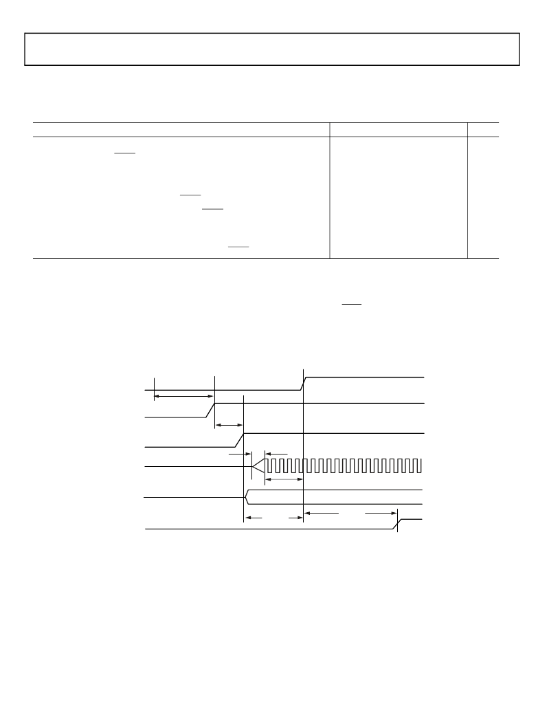
Power-Up Sequencing
The timing requirements for DSP startup are given in
Table 9
.
Table 9. Power-Up Sequencing Timing Requirements (DSP Startup)
Parameter
Min
Max
Unit
Timing Requirements
t
RSTVDD
t
IVDDEVDD
t
CLKVDD
t
CLKRST
t
PLLRST
RESET Low Before V
DDINT
/V
DDEXT
on
V
DDINT
on Before V
DDEXT
CLKIN Valid After V
DDINT
/V
DDEXT
valid
1
CLKIN Valid Before RESET Deasserted
0
ns
–50
200
ms
0
10
2
20
3
200
ms
μs
PLL Control Setup Before RESET Deasserted
μs
Switching Characteristic
t
CORERST
DSP Core Reset Deasserted After RESET Deasserted
4096t
CK4,
5
1
Valid V
/V
assumes that the supplies are fully ramped to their 1.2 and 3.3 volt rails. Voltage ramp rates can vary from microseconds to hundreds of milliseconds
depending on the design of the power supply subsystem.
2
Assumes a stable CLKIN signal, after meeting worst-case startup timing of crystal oscillators. Refer to the crystal oscillator manufacturer's data sheet for startup time.
Assume a 25 ms maximum oscillator startup time if using the XTAL pin and internal oscillator circuit in conjunction with an external crystal.
3
Based on CLKIN cycles.
4
Applies after the power-up sequence is complete. Subsequent resets require a minimum of 4 CLKIN cycles for RESET to be held low in order to properly initialize and
propagate default states at all I/O pins.
5
The 4096 cycle count depends on t
SRST
specification in
Table 11
. If setup time is not met, 1 additional CLKIN cycle may be added to the core reset time, resulting in 4097
cycles maximum.
Figure 6. Power-Up Sequencing
CLKIN
RESET
t
RSTVDD
RSTOUT*
VDDEXT
VDDINT
t
PLLRST
t
CLKRST
t
CLKVDD
t
IVDDEVDD
CLK_CFG1-0
t
CO RERST
*MULTIPLEXED WITH CLKOUT
相關(guān)PDF資料 |
PDF描述 |
|---|---|
| ADSP-21262 | SHARC Processor |
| ADSP-21262SKBC-200 | SHARC Processor |
| ADSP-21262SKBCZ200 | SHARC Processor |
| ADSP-21266 | SHARC Embedded Processor |
| ADSP-21266SKBC-2B | SHARC Embedded Processor |
相關(guān)代理商/技術(shù)參數(shù) |
參數(shù)描述 |
|---|---|
| ADSP-21262SKSTZ200 | 制造商:Analog Devices 功能描述:IC 32-BIT DSP |
| ADSP-21266 | 制造商:AD 制造商全稱:Analog Devices 功能描述:SHARC Embedded Processor |
| ADSP-21266_07 | 制造商:AD 制造商全稱:Analog Devices 功能描述:Embedded Processor |
| ADSP-21266KSTZ-1C | 制造商:Analog Devices 功能描述:- Trays |
| ADSP-21266KSTZ-2C | 制造商:Analog Devices 功能描述:- Trays |
發(fā)布緊急采購(gòu),3分鐘左右您將得到回復(fù)。