- 您現(xiàn)在的位置:買賣IC網(wǎng) > PDF目錄383961 > TMX320DM6443AZWT (Texas Instruments, Inc.) Digital Media System-on-Chip PDF資料下載
參數(shù)資料
| 型號(hào): | TMX320DM6443AZWT |
| 廠商: | Texas Instruments, Inc. |
| 英文描述: | Digital Media System-on-Chip |
| 中文描述: | 數(shù)字媒體系統(tǒng)片上 |
| 文件頁數(shù): | 190/221頁 |
| 文件大小: | 1582K |
| 代理商: | TMX320DM6443AZWT |
第1頁第2頁第3頁第4頁第5頁第6頁第7頁第8頁第9頁第10頁第11頁第12頁第13頁第14頁第15頁第16頁第17頁第18頁第19頁第20頁第21頁第22頁第23頁第24頁第25頁第26頁第27頁第28頁第29頁第30頁第31頁第32頁第33頁第34頁第35頁第36頁第37頁第38頁第39頁第40頁第41頁第42頁第43頁第44頁第45頁第46頁第47頁第48頁第49頁第50頁第51頁第52頁第53頁第54頁第55頁第56頁第57頁第58頁第59頁第60頁第61頁第62頁第63頁第64頁第65頁第66頁第67頁第68頁第69頁第70頁第71頁第72頁第73頁第74頁第75頁第76頁第77頁第78頁第79頁第80頁第81頁第82頁第83頁第84頁第85頁第86頁第87頁第88頁第89頁第90頁第91頁第92頁第93頁第94頁第95頁第96頁第97頁第98頁第99頁第100頁第101頁第102頁第103頁第104頁第105頁第106頁第107頁第108頁第109頁第110頁第111頁第112頁第113頁第114頁第115頁第116頁第117頁第118頁第119頁第120頁第121頁第122頁第123頁第124頁第125頁第126頁第127頁第128頁第129頁第130頁第131頁第132頁第133頁第134頁第135頁第136頁第137頁第138頁第139頁第140頁第141頁第142頁第143頁第144頁第145頁第146頁第147頁第148頁第149頁第150頁第151頁第152頁第153頁第154頁第155頁第156頁第157頁第158頁第159頁第160頁第161頁第162頁第163頁第164頁第165頁第166頁第167頁第168頁第169頁第170頁第171頁第172頁第173頁第174頁第175頁第176頁第177頁第178頁第179頁第180頁第181頁第182頁第183頁第184頁第185頁第186頁第187頁第188頁第189頁當(dāng)前第190頁第191頁第192頁第193頁第194頁第195頁第196頁第197頁第198頁第199頁第200頁第201頁第202頁第203頁第204頁第205頁第206頁第207頁第208頁第209頁第210頁第211頁第212頁第213頁第214頁第215頁第216頁第217頁第218頁第219頁第220頁第221頁
www.ti.com
SPI_CLK
(Clock Polarity = 0)
SPI_CLK
(Clock Polarity = 1)
SPI_DI
(Input)
SPI_DO
(Output)
4
MSB IN
DATA
LSB IN
LSB OUT
MSB OUT
DATA
9
10
8
6
5
7
SPI_EN
11
TMS320DM6443
Digital Media System-on-Chip
SPRS282E–DECEMBER 2005–REVISED MARCH 2007
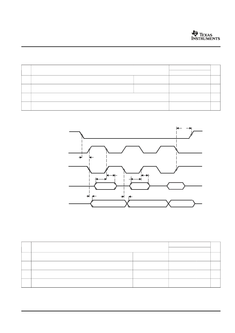
Table 6-74. Switching Characteristics Over Recommended Operating Conditions for SPI Master Mode
[Clock Phase = 0] (see
Figure 6-59
)
-594
MIN
NO.
PARAMETER
UNIT
MAX
Delay time, SPI_CLK (output) rising edge to SPI_DO
(output) transition
Delay time, SPI_CLK (output) falling edge to SPI_DO
(output) transition
Delay time, SPI_EN[1:0] (output) falling edge to first SPI_CLK (output) rising or
falling edge
(1)(2)
Delay time, SPI_CLK (output) rising or falling edge to SPI_EN[1:0] (output)
rising edge
(1)(2)(3)
8
t
d(CLKH-DOV)
Clock Polarity = 0
-4
5
ns
9
t
d(CLKL-DOV)
Clock Polarity = 1
-4
5
ns
10
t
d(ENL-CLKH/L)
2P - 2.3
ns
11
t
d(CLKH/L-ENH)
1P + 0.5C - 0.2
ns
(1)
(2)
(3)
P = Period of the SPI module clock in nanoseconds (SYSCLK5).
This delay can be increased under software control by the C2TDELAY register bit field in the SPIDELAY register.
C = Period of SPI_CLK signal in ns.
Figure 6-59. SPI Master Mode External Timing (Clock Phase = 0)
6.17.2.2
SPI Master Mode Timings (Clock Phase = 1)
Table 6-75. Timing Requirements for SPI Master Mode [Clock Phase = 1]
(1)
(see
Figure 6-60
)
-594
MIN
NO.
UNIT
MAX
Setup time, SPI_DI (input) valid before SPI_CLK
(output) rising edge
Setup time, SPI_DI (in put) valid before SPI_CLK
(output) falling edge
Hold time, SPI_DI (input) valid after SPI_CLK (output)
rising edge
Hold time, SPI_DI (input) valid after SPI_CLK (output)
falling edge
13
t
su(DIV-CLKL)
Clock Polarity = 0
0.5P + 9.4
ns
14
t
su(DIV-CLKH)
Clock Polarity = 1
0.5P + 9.4
ns
15
t
h(CLKL-DIV)
Clock Polarity = 0
0.5P - 4.5
ns
16
t
h(CLKH-DIV)
Clock Polarity = 1
0.5P - 4.5
ns
(1)
P = Period of the SPI module clock in nanoseconds (SYSCLK5).
Peripheral and Electrical Specifications
190
Submit Documentation Feedback
相關(guān)PDF資料 |
PDF描述 |
|---|---|
| TMX320DM6443ZWT | Digital Media System-on-Chip |
| TMS320DM647_08 | Digital Media Processor |
| TMS320DM647ZUT720 | Digital Media Processor |
| TMS320DM647ZUT900 | Digital Media Processor |
| TMS320DM648ZUT720 | Digital Media Processor |
相關(guān)代理商/技術(shù)參數(shù) |
參數(shù)描述 |
|---|---|
| TMX320DM6443BZWT | 制造商:Texas Instruments 功能描述: |
| TMX320DM6443CZWT | 制造商:Texas Instruments 功能描述: |
| TMX320DM6443ZWT | 制造商:Texas Instruments 功能描述: |
| TMX320DM6444AZWT | 制造商:Texas Instruments 功能描述:TMS320DM6443, TMS320DM6444 DIGITAL MEDIA SOC DATA SHEET - Trays |
| TMX320DM6446AZWT | 制造商:Texas Instruments 功能描述: |
發(fā)布緊急采購,3分鐘左右您將得到回復(fù)。