- 您現(xiàn)在的位置:買賣IC網(wǎng) > PDF目錄383876 > T7237A Compliance with the New ETSI PSD Requirement PDF資料下載
參數(shù)資料
| 型號(hào): | T7237A |
| 英文描述: | Compliance with the New ETSI PSD Requirement |
| 中文描述: | 符合新的ETSI PSD的要求 |
| 文件頁數(shù): | 63/116頁 |
| 文件大?。?/td> | 1056K |
| 代理商: | T7237A |
第1頁第2頁第3頁第4頁第5頁第6頁第7頁第8頁第9頁第10頁第11頁第12頁第13頁第14頁第15頁第16頁第17頁第18頁第19頁第20頁第21頁第22頁第23頁第24頁第25頁第26頁第27頁第28頁第29頁第30頁第31頁第32頁第33頁第34頁第35頁第36頁第37頁第38頁第39頁第40頁第41頁第42頁第43頁第44頁第45頁第46頁第47頁第48頁第49頁第50頁第51頁第52頁第53頁第54頁第55頁第56頁第57頁第58頁第59頁第60頁第61頁第62頁當(dāng)前第63頁第64頁第65頁第66頁第67頁第68頁第69頁第70頁第71頁第72頁第73頁第74頁第75頁第76頁第77頁第78頁第79頁第80頁第81頁第82頁第83頁第84頁第85頁第86頁第87頁第88頁第89頁第90頁第91頁第92頁第93頁第94頁第95頁第96頁第97頁第98頁第99頁第100頁第101頁第102頁第103頁第104頁第105頁第106頁第107頁第108頁第109頁第110頁第111頁第112頁第113頁第114頁第115頁第116頁
Data Sheet
January 1998
T7256 Single-Chip NT1 (SCNT1) Transceiver
Lucent Technologies Inc.
59
Application Briefs
(continued)
Using the T7256 in a Combination TE/TA
Environment (NT1/TA)
The T7256 can be used in applications requiring NT1
and terminal adapter (TA) functionality (NT1/TA). This
application brief describes an NT1 that supports con-
ventional POTS (plain old telephone service) as well as
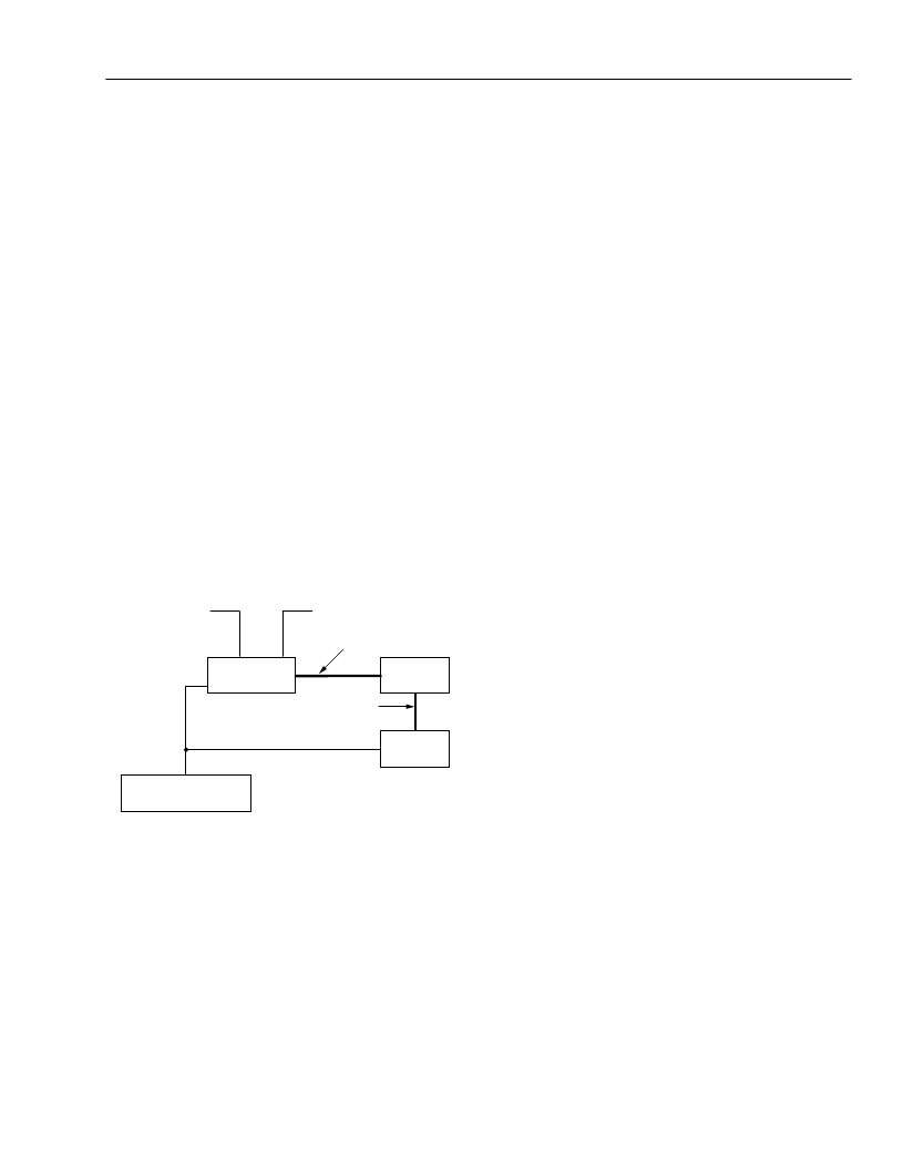
ISDN service. A block diagram of this application is
shown in Figure 22. The microprocessor (
μ
P) performs
the following functions:
I
Runs the ISDN call control stack (Q.931).
I
Controls the HDLC formatter for performing the
LAP-D protocol on the D channel.
I
Controls the register configuration of the T7256.
I
Controls the POTS circuitry (i.e., translates signaling
such as off-hook into the correct call-control mes-
sage, translates DTMF digits from a DTMF receiver,
controls the ringer, etc.).
I
Controls access to the B and D channels on the TDM
highway for the codecs and HDLC formatter, respec-
tively.
5-3646(C).b
Figure 22. T7256 NT1/TA Application Block Diagram
T7256 Configuration
When the T7256 is used in the NT1/TA application, the
TDM highway must be used in conjunction with the
data flow control registers (DFR0 and DFR1) to control
the B- and D-channel data flow. Following is a sug-
gested procedure for properly configuring the T7256 in
this application.
1. Set TDMEN = 0 (register GR2, bit 5) to enable the
TDM highway. In this case, the ps1/ps2 functions
must be controlled via the microprocessor (register
GR1, bits 1 and 2) because pins 8 and 9 are used
for TDMDO and TDMCLK. Note that when the TDM
highway is enabled, TDMCLK and FS will not
become active until at least one of the bits 2—7 in
register DFR1 are enabled (set to 0).
2. The downstream D channel must be monitored by
the TA circuit for call-control messages from the
switch. This is accomplished via the TDM bus by
setting TDMDU = 0 (register DFR1, bit 7). The
upstream D channel (which is normally sourced
from the S/T-interface) must be sourced by the
POTS HDLC controller when one of the following
events occurs:
a. The switch notifies the POTS circuit of an incom-
ing call request via a downstream D-channel
message.
b. A local POTS phone goes off-hook (i.e., a call is
being placed).
In either of these cases, the POTS HDLC controller
must take control of the D-channel in order to com-
plete the call setup for the appropriate POTS phone.
This is accomplished by setting UXD = 0 (register
DFR1, bit 0).
3. The frame strobe pulse envelope and polarity must
be configured for correct operation with the HDLC
controller and codecs using register TDR0. For
example, to set an active-high FS pulse that enve-
lopes the U-interface B1 channel data (see Figure
18), register TDR0 bits 0—3 should be set to all 1s
(default on powerup). This setting can be used with
the Lucent T7121 HDLC controller because the
T7121 can be programmed for any time slot and bit
offset from the rising or falling edge of FS.
The codecs may require the FS pulse be in a partic-
ular position relative to the B-channel data. For
example, if two Lucent T7513B codecs are used in
variable timing mode in this application (one for
each POTS line), each would require an FS pulse
that envelopes the appropriate B-channel data. The
configuration described in the preceding paragraph
is adequate for allowing either codec to source or
sink B1 channel data to the U-interface, but there is
no separate FS pulse available for the B2 channel
data. Therefore, external glue logic is necessary to
generate an FS pulse for the B2 channel data.
T7256
U-INTERFACE
SERIAL INTERFACE
μP
PARALLEL INTERFACE
HDLC
CODEC,
SLICS, RINGERS, DTMF
RECEIVERS, ETC.
TDM HIGHWAYS
S/T-INTERFACE
相關(guān)PDF資料 |
PDF描述 |
|---|---|
| T7256A | Compliance with the New ETSI PSD Requirement |
| T7288 | CEPT/E1 Line Interface(CEPT/E1 線接口) |
| T7290A | DS1/T1/CEPT/E1 Line Interface(DS1/T1/CEPT/E1 線接口) |
| T7295-1 | E3 Integrated Line Receiver(E3 集成線接收器) |
| T7295-6 | DS3/SONET STS-1 Integrated Line Receiver(DS3/SONET STS-1 集成線接收器) |
相關(guān)代理商/技術(shù)參數(shù) |
參數(shù)描述 |
|---|---|
| T7240 | 制造商:TE Connectivity 功能描述: |
| T7-241A5 | 功能描述:撥動(dòng)開關(guān) ON NONE OFF 2 Pole Standard Bat Handle RoHS:否 制造商:OTTO 觸點(diǎn)形式: 開關(guān)功能: 電流額定值: 電壓額定值 AC: 電壓額定值 DC: 功率額定值: 端接類型: 安裝風(fēng)格: 端子密封: 觸點(diǎn)電鍍: 照明: |
| T7-241B1 | 制造商:OTTO 功能描述:Toggle Switches ON NONE ON 2 Pole Standard Bat Handle 制造商:OTTO Engineering Inc 功能描述:Switch Toggle ON None ON DPDT Bat Toggle PC Pins 16A 115VAC 28VDC PC Mount with Threads |
| T7-241B5 | 功能描述:撥動(dòng)開關(guān) ON NONE ON 2 Pole Standard Bat Handle RoHS:否 制造商:OTTO 觸點(diǎn)形式: 開關(guān)功能: 電流額定值: 電壓額定值 AC: 電壓額定值 DC: 功率額定值: 端接類型: 安裝風(fēng)格: 端子密封: 觸點(diǎn)電鍍: 照明: |
| T7-241C5 | 制造商:OTTO 功能描述:Toggle Switches (ON) NONE OFF 2 Pole Standard Bat Handle 制造商:OTTO Engineering Inc 功能描述:Switch Toggle (ON) None OFF DPST Bat Toggle PC Pins 16A 115VAC 28VDC PC Mount with Threads |
發(fā)布緊急采購(gòu),3分鐘左右您將得到回復(fù)。