- 您現(xiàn)在的位置:買賣IC網(wǎng) > PDF目錄385814 > SAA7712 (NXP Semiconductors N.V.) Sound effects DSP PDF資料下載
參數(shù)資料
| 型號(hào): | SAA7712 |
| 廠商: | NXP Semiconductors N.V. |
| 英文描述: | Sound effects DSP |
| 中文描述: | DSP的音效 |
| 文件頁數(shù): | 7/44頁 |
| 文件大小: | 178K |
| 代理商: | SAA7712 |
第1頁第2頁第3頁第4頁第5頁第6頁當(dāng)前第7頁第8頁第9頁第10頁第11頁第12頁第13頁第14頁第15頁第16頁第17頁第18頁第19頁第20頁第21頁第22頁第23頁第24頁第25頁第26頁第27頁第28頁第29頁第30頁第31頁第32頁第33頁第34頁第35頁第36頁第37頁第38頁第39頁第40頁第41頁第42頁第43頁第44頁
1999 Aug 05
7
Philips Semiconductors
Preliminary specification
Sound effects DSP
SAA7712H
7
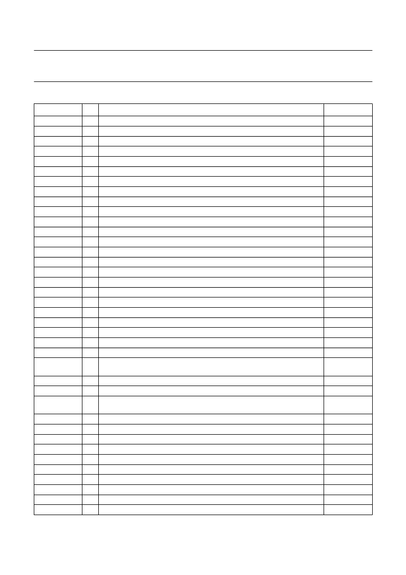
PINNING INFORMATION
SYMBOL
PIN
DESCRIPTION
PIN TYPE
n.c.
n.c.
n.c.
n.c.
n.c.
n.c.
n.c.
POM
OUT3_V
OUT3_I
OUT2_I
OUT2_V
V
SSA2
V
DDA2
VREFDA
OUT1_V
OUT1_I
OUT0_I
OUT0_V
EQOV
SYS_CLK
V
DDD5V1
V
SSD5V1
I
2
S_IN2_WS
I
2
S_IN2_DATA
1
2
3
4
5
6
7
8
9
10
11
12
13
14
15
16
17
18
19
20
21
22
23
24
25
not connected
not connected
not connected
not connected
not connected
not connected
not connected
power-on mute; timing determined by external capacitor
analog voltage output 3
analog current output 3
analog current output 2
analog voltage output 2
analog ground supply 2
analog supply voltage 2 (3 V)
voltage reference of the analog part
analog voltage output 1
analog current output 1
analog current output 0
analog voltage output 0
equalizer overflow line output
test pin output
digital supply voltage 1; peripheral cells only (3 or 5 V)
digital ground supply 1; peripheral cells only (3 or 5 V)
I
2
S-bus or LSB-justified format word select input from a digital audio source 2
I
2
S-bus or LSB-justified format left-right data input from a digital audio
source 2
I
2
S-bus clock or LSB-justified format input from a digital audio source 2
I
2
S-bus or LSB-justified format word select input from a digital audio source 1
I
2
S-bus or LSB-justified format left-right data input from a digital audio
source 1
I
2
S-bus clock or LSB-justified format input from a digital audio source 1
I
2
S-bus bit clock output for interface with DSP co-processor chip
I
2
S-bus input data channel 1 from DSP co-processor chip
I
2
S-bus input data channel 2 from DSP co-processor chip
I
2
S-bus word select output for interface with DSP co-processor chip
digital supply voltage 2; peripheral cells only (3 or 5 V)
digital ground supply 2; peripheral cells only (3 or 5 V)
I
2
S-bus output data channel 1 to DSP co-processor chip
I
2
S-bus output data channel 2 to DSP co-processor chip
digital input 1 of the DSP core (F0 of the status register)
AP2D
AP2D
AP2D
AP2D
AP2D
APVSS
APVDD
AP2D
AP2D
AP2D
AP2D
AP2D
B4CR
BT4CR
VDD5
VSS5
IBUFD
IBUFD
I
2
S_IN2_BCK
I
2
S_IN1_WS
I
2
S_IN1_DATA
26
27
28
IBUFD
IBUFD
IBUFD
I
2
S_IN1_BCK
I
2
S_IO_BCK
I
2
S_IO_IN1
I
2
S_IO_IN2
I
2
S_IO_WS
V
DDD5V2
V
SSD5V2
I
2
S_IO_OUT1
I
2
S_IO_OUT2
DSP_IN1
29
30
31
32
33
34
35
36
37
38
IBUFD
BT4CR
IBUFD
IBUFD
BT4CR
VDD5
VSS5
BT4CR
BT4CR
IBUFD
相關(guān)PDF資料 |
PDF描述 |
|---|---|
| SAA8110G | Digital Signal Processor (DSP) for cameras(應(yīng)用于照相中的數(shù)字信號(hào)處理器) |
| SAA8122A | Digital Still Camera Processor (ImagIC family)(數(shù)字靜態(tài)照相處理器) |
| SAA8122AEL | Digital Still Camera Processor ImagIC family |
| SAB-C504-2R24M | 8-Bit CMOS Microcontroller |
| SAB-C504-2R40M | 8-Bit CMOS Microcontroller |
相關(guān)代理商/技術(shù)參數(shù) |
參數(shù)描述 |
|---|---|
| SAA7712H | 制造商:PHILIPS 制造商全稱:NXP Semiconductors 功能描述:Sound effects DSP |
| SAA7715 | 制造商:PHILIPS 制造商全稱:NXP Semiconductors 功能描述:Digital Signal Processor |
| SAA7715H | 制造商:PHILIPS 制造商全稱:NXP Semiconductors 功能描述:Digital Signal Processor |
| SAA7724H | 制造商:PHILIPS 制造商全稱:NXP Semiconductors 功能描述:Car radio digital signal processor |
| SAA7740 | 制造商:PHILIPS 制造商全稱:NXP Semiconductors 功能描述:Digital Audio Processing IC DAPIC |
發(fā)布緊急采購,3分鐘左右您將得到回復(fù)。