- 您現(xiàn)在的位置:買賣IC網(wǎng) > PDF目錄98069 > S1C88317D0A0100 MICROCONTROLLER, UUC170 PDF資料下載
參數(shù)資料
| 型號: | S1C88317D0A0100 |
| 元件分類: | 微控制器/微處理器 |
| 英文描述: | MICROCONTROLLER, UUC170 |
| 封裝: | DIE-170 |
| 文件頁數(shù): | 245/343頁 |
| 文件大小: | 2396K |
| 代理商: | S1C88317D0A0100 |
第1頁第2頁第3頁第4頁第5頁第6頁第7頁第8頁第9頁第10頁第11頁第12頁第13頁第14頁第15頁第16頁第17頁第18頁第19頁第20頁第21頁第22頁第23頁第24頁第25頁第26頁第27頁第28頁第29頁第30頁第31頁第32頁第33頁第34頁第35頁第36頁第37頁第38頁第39頁第40頁第41頁第42頁第43頁第44頁第45頁第46頁第47頁第48頁第49頁第50頁第51頁第52頁第53頁第54頁第55頁第56頁第57頁第58頁第59頁第60頁第61頁第62頁第63頁第64頁第65頁第66頁第67頁第68頁第69頁第70頁第71頁第72頁第73頁第74頁第75頁第76頁第77頁第78頁第79頁第80頁第81頁第82頁第83頁第84頁第85頁第86頁第87頁第88頁第89頁第90頁第91頁第92頁第93頁第94頁第95頁第96頁第97頁第98頁第99頁第100頁第101頁第102頁第103頁第104頁第105頁第106頁第107頁第108頁第109頁第110頁第111頁第112頁第113頁第114頁第115頁第116頁第117頁第118頁第119頁第120頁第121頁第122頁第123頁第124頁第125頁第126頁第127頁第128頁第129頁第130頁第131頁第132頁第133頁第134頁第135頁第136頁第137頁第138頁第139頁第140頁第141頁第142頁第143頁第144頁第145頁第146頁第147頁第148頁第149頁第150頁第151頁第152頁第153頁第154頁第155頁第156頁第157頁第158頁第159頁第160頁第161頁第162頁第163頁第164頁第165頁第166頁第167頁第168頁第169頁第170頁第171頁第172頁第173頁第174頁第175頁第176頁第177頁第178頁第179頁第180頁第181頁第182頁第183頁第184頁第185頁第186頁第187頁第188頁第189頁第190頁第191頁第192頁第193頁第194頁第195頁第196頁第197頁第198頁第199頁第200頁第201頁第202頁第203頁第204頁第205頁第206頁第207頁第208頁第209頁第210頁第211頁第212頁第213頁第214頁第215頁第216頁第217頁第218頁第219頁第220頁第221頁第222頁第223頁第224頁第225頁第226頁第227頁第228頁第229頁第230頁第231頁第232頁第233頁第234頁第235頁第236頁第237頁第238頁第239頁第240頁第241頁第242頁第243頁第244頁當(dāng)前第245頁第246頁第247頁第248頁第249頁第250頁第251頁第252頁第253頁第254頁第255頁第256頁第257頁第258頁第259頁第260頁第261頁第262頁第263頁第264頁第265頁第266頁第267頁第268頁第269頁第270頁第271頁第272頁第273頁第274頁第275頁第276頁第277頁第278頁第279頁第280頁第281頁第282頁第283頁第284頁第285頁第286頁第287頁第288頁第289頁第290頁第291頁第292頁第293頁第294頁第295頁第296頁第297頁第298頁第299頁第300頁第301頁第302頁第303頁第304頁第305頁第306頁第307頁第308頁第309頁第310頁第311頁第312頁第313頁第314頁第315頁第316頁第317頁第318頁第319頁第320頁第321頁第322頁第323頁第324頁第325頁第326頁第327頁第328頁第329頁第330頁第331頁第332頁第333頁第334頁第335頁第336頁第337頁第338頁第339頁第340頁第341頁第342頁第343頁
S1C88348/317/316/308 TECHNICAL SOFTWARE
EPSON
II-111
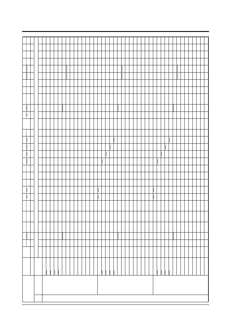
APPENDIX A TABLE OF INPUT/OUTPUT PORT TERMINALS
Appendix A
Table of Input/Output Port Terminals
CPU
mode
Bus
mode
K00~07
K10
K11
R
00~07
R10~17
R20~22
R23
R24
(Initial
setting)
CE0
output
(invalid)
CE1
output
(invalid)
CE2
output
(invalid)
CE3
output
(invalid)
Bus
release
Serial
interface
Comparator
0
Comparator
1
CL
output
FR
output
TOUT
output
FOUT
output
BZ
output
Single
chip
Expanded
64K
Expanded
512K
(MIN
&
MAX)
MCU
Input
port
terminals
Special
output
R25
R26
R27
R30
R31
R32
R33
R34
R35~37
R50
R51
P00~07
P10
P11
P12
P13
P14
P15
P16
P17
Output
port
terminals
I/O
port
terminals
K00~07
K10
K
11
↑
BREQ
R00~07
R10~17
R20~22
R23
R24
R25
R26
R27
R30
R31
R32
R33
R34
R35~37
R50
R51
↑
CL
FR
TOUT
FOUT
BZ
BACK
P00~07
P10
P11
P12
P13
P14
P15
P16
P17
↑
S
IN
SOUT
SCLK
S
R
D
Y
CMPP0
CMPM0
CMPP1
CMPM1
(No
special
output)
CE0
output
CE1
output
CE2
output
CE3
output
Bus
release
Serial
interface
Comparator
0
Comparator
1
CL
output
FR
output
TOUT
output
FOUT
output
BZ
output
K00~07
K10
K
11
↑
BREQ
A0~7
A8~15
R20~22
RD
WR
R25
R
26
R27
R
30
R31
R
32
R33
R
34
R35~37
R50
R
51
↑
CL
FR
TOUT
FOUT
BZ
BACK
D0~7
P10
P11
P12
P13
P14
P15
P16
P17
↑
S
IN
SOUT
SCLK
S
R
D
Y
CMPP0
CMPM0
CMPP1
CMPM1
(No
special
output)
CE0
output
CE1
output
CE2
output
CE3
output
Bus
release
Serial
interface
Comparator
0
Comparator
1
CL
output
FR
output
TOUT
output
FOUT
output
BZ
output
K00~07
K10
K
11
↑
BREQ
A0~7
A8~15
A16~18
RD
WR
R25
R
26
R27
R
30
R31
R
32
R33
R
34
R35~37
R50
R
51
↑
CL
FR
TOUT
FOUT
BZ
BACK
D0~7
P10
P11
P12
P13
P14
P15
P16
P17
↑
S
IN
SOUT
SCLK
S
R
D
Y
CMPP0
CMPM0
CMPP1
CMPM1
CE0
CE1
CE2
CE3
CE0
CE1
CE2
CE3
Terminal
configuration
depending
on
model
S1C88308
S1C88348 S1C88317 S1C88316
P00~07
D0~7
P10
SIN
P11
P12
SCLK
P13
P
14
P15
P
16
P17
↑
↑↑↑↑
↑↑↑
R27
TOUT
R30
CE0
R31
CE1
R32
CE2
R33
CE3
R34
FOUT
R35~37
R50
BZ
R51
BACK
↑↑↑↑↑↑
↑
R00~07
A0~7
R10~17
A8~15
R20~22
A16~18
R23
RD
R24
WR
R25
CL
R26
FR
↑
↑↑↑↑
K00~07
K10
EVIN
K11
BREQ
↑↑
SOUT
SRDY
CMPP0
CMPM0
CMPP1
CMPM1
相關(guān)PDF資料 |
PDF描述 |
|---|---|
| S1C88308D0A0100 | MICROCONTROLLER, UUC170 |
| S1C88308F0A0100 | MICROCONTROLLER, PQFP160 |
| S1C88348F | 8-BIT, MROM, 8.2 MHz, MICROCONTROLLER, PQFP16 |
| S1C88316D | 8-BIT, MROM, 8.2 MHz, MICROCONTROLLER, UUC172 |
| S1C88316F | 8-BIT, MROM, 8.2 MHz, MICROCONTROLLER, PQFP16 |
相關(guān)代理商/技術(shù)參數(shù) |
參數(shù)描述 |
|---|---|
| S1C88349 | 制造商:EPSON 制造商全稱:EPSON 功能描述:8-bit Single Chip Microcomputer |
| S1C88649 | 制造商:EPSON 制造商全稱:EPSON 功能描述:8-bit Single Chip Microcomputer |
| S1C88650 | 制造商:EPSON 制造商全稱:EPSON 功能描述:8-bit Single Chip Microcomputer |
| S1C88655 | 制造商:EPSON 制造商全稱:EPSON 功能描述:8-bit Single Chip Microcomputer |
| S1C88816 | 制造商:EPSON 制造商全稱:EPSON 功能描述:8-bit Single Chip Microcomputer |
發(fā)布緊急采購,3分鐘左右您將得到回復(fù)。