- 您現(xiàn)在的位置:買賣IC網(wǎng) > PDF目錄383740 > PFR4200MPB40 (飛思卡爾半導體(中國)有限公司) FlexRay Communication Controllers PDF資料下載
參數(shù)資料
| 型號: | PFR4200MPB40 |
| 廠商: | 飛思卡爾半導體(中國)有限公司 |
| 英文描述: | FlexRay Communication Controllers |
| 中文描述: | FlexRay通信控制器 |
| 文件頁數(shù): | 223/260頁 |
| 文件大小: | 1782K |
| 代理商: | PFR4200MPB40 |
第1頁第2頁第3頁第4頁第5頁第6頁第7頁第8頁第9頁第10頁第11頁第12頁第13頁第14頁第15頁第16頁第17頁第18頁第19頁第20頁第21頁第22頁第23頁第24頁第25頁第26頁第27頁第28頁第29頁第30頁第31頁第32頁第33頁第34頁第35頁第36頁第37頁第38頁第39頁第40頁第41頁第42頁第43頁第44頁第45頁第46頁第47頁第48頁第49頁第50頁第51頁第52頁第53頁第54頁第55頁第56頁第57頁第58頁第59頁第60頁第61頁第62頁第63頁第64頁第65頁第66頁第67頁第68頁第69頁第70頁第71頁第72頁第73頁第74頁第75頁第76頁第77頁第78頁第79頁第80頁第81頁第82頁第83頁第84頁第85頁第86頁第87頁第88頁第89頁第90頁第91頁第92頁第93頁第94頁第95頁第96頁第97頁第98頁第99頁第100頁第101頁第102頁第103頁第104頁第105頁第106頁第107頁第108頁第109頁第110頁第111頁第112頁第113頁第114頁第115頁第116頁第117頁第118頁第119頁第120頁第121頁第122頁第123頁第124頁第125頁第126頁第127頁第128頁第129頁第130頁第131頁第132頁第133頁第134頁第135頁第136頁第137頁第138頁第139頁第140頁第141頁第142頁第143頁第144頁第145頁第146頁第147頁第148頁第149頁第150頁第151頁第152頁第153頁第154頁第155頁第156頁第157頁第158頁第159頁第160頁第161頁第162頁第163頁第164頁第165頁第166頁第167頁第168頁第169頁第170頁第171頁第172頁第173頁第174頁第175頁第176頁第177頁第178頁第179頁第180頁第181頁第182頁第183頁第184頁第185頁第186頁第187頁第188頁第189頁第190頁第191頁第192頁第193頁第194頁第195頁第196頁第197頁第198頁第199頁第200頁第201頁第202頁第203頁第204頁第205頁第206頁第207頁第208頁第209頁第210頁第211頁第212頁第213頁第214頁第215頁第216頁第217頁第218頁第219頁第220頁第221頁第222頁當前第223頁第224頁第225頁第226頁第227頁第228頁第229頁第230頁第231頁第232頁第233頁第234頁第235頁第236頁第237頁第238頁第239頁第240頁第241頁第242頁第243頁第244頁第245頁第246頁第247頁第248頁第249頁第250頁第251頁第252頁第253頁第254頁第255頁第256頁第257頁第258頁第259頁第260頁
General
MFR4200 Data Sheet, Rev. 0
Freescale Semiconductor
223
A.1.7
Operating Conditions
This chapter describes the operating conditions of the device. Unless otherwise noted those conditions
apply to all the following data.
NOTE
Refer to the temperature rating of the device (C, V, M) with regards to the
ambient temperature T
A
and the junction temperature T
J
. For power
dissipation calculations refer to
Section A.1.8, “Power Dissipation and
Thermal Characteristics
”.
A.1.8
Power Dissipation and Thermal Characteristics
Power dissipation and thermal characteristics are closely related. The user must assure that the maximum
operating junction temperature is not exceeded. The average chip-junction temperature (T
J
) in
°
C can be
obtained from:
Eqn. A-1
T
J
= Junction Temperature [°C]
T
A
= Ambient Temperature [°C]
P
D
= Total Chip Power Dissipation [W]
Θ
JA
= Package Thermal Resistance [°C/W]
The total power dissipation can be calculated from:
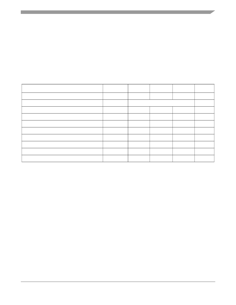
Table A-4. Operating Conditions
Rating
Symbol
Min
Typ
Max
Unit
Oscillator and Quartz frequency
f
OSC
-
40.000
40.000
MHz
Quartz overtone
Fundamental Frequency
Quartz frequency stability at T
J
f
STB
-1500
300
1500
ppm
Voltage difference VDDX to VDDR and VDDA
D
VDDX
-0.1
0
0.1
V
Voltage difference VSSX to VSSR and VSSA
D
VSSX
-0.1
0
0.1
V
I/O, Regulator and Analog Supply
V
DD5
2.97
3.3
5.5
V
Digital Logic Supply Voltage
1
1
The device contains an internal voltage regulator to generate the logic and OSC supply out of the I/O supply.
2
Refer to
Section A.1.8, “Power Dissipation and Thermal Characteristics
” for more information about the relation between
ambient temperature T
A
and device junction temperature T
J
.
V
DD
2.25
2.5
2.75
V
Oscillator Supply Voltage
1
V
DDOSC
2.25
2.5
2.75
V
Operating Junction Temperature Range
T
J
-40
-
140
o
C
Operating Ambient Temperature Range
2
T
J
-40
27
125
o
C
TJ
TA
PD
Θ
JA
(
)
+
=
相關PDF資料 |
PDF描述 |
|---|---|
| PFR850S | FAST RECOVERY RECTIFIER DIODES |
| PFR851S | FAST RECOVERY RECTIFIER DIODES |
| PFR852S | FAST RECOVERY RECTIFIER DIODES |
| PFR853S | FAST RECOVERY RECTIFIER DIODES |
| PFR854S | FAST RECOVERY RECTIFIER DIODES |
相關代理商/技術參數(shù) |
參數(shù)描述 |
|---|---|
| PFR4310E1MAE40 | 制造商:Freescale Semiconductor 功能描述: |
| PFR4KR100E | 制造商:OHMITE 制造商全稱:Ohmite Mfg. Co. 功能描述:Powr-Rib Edgewound Edgewound and Round Wire |
| PFR5 102J630J11L4 | 制造商:Evox Rifa / KEMET 功能描述:PULSE CAP 0.001UF 630VDC |
| PFR5 102J63J11L4 | 制造商:Evox Rifa / KEMET 功能描述:PULSE CAP 0.001UF 63VDC |
| PFR5 103J63J12L4 | 制造商:Evox Rifa / KEMET 功能描述:PULSE CAP 0.01UF 63VDC |
發(fā)布緊急采購,3分鐘左右您將得到回復。