- 您現(xiàn)在的位置:買賣IC網(wǎng) > PDF目錄299581 > ORT82G5-1BM680 (LATTICE SEMICONDUCTOR CORP) FPGA, 1296 CLBS, 380000 GATES, PBGA680 PDF資料下載
參數(shù)資料
| 型號: | ORT82G5-1BM680 |
| 廠商: | LATTICE SEMICONDUCTOR CORP |
| 元件分類: | FPGA |
| 英文描述: | FPGA, 1296 CLBS, 380000 GATES, PBGA680 |
| 封裝: | PLASTIC, BGA-680 |
| 文件頁數(shù): | 46/110頁 |
| 文件大小: | 1459K |
| 代理商: | ORT82G5-1BM680 |
第1頁第2頁第3頁第4頁第5頁第6頁第7頁第8頁第9頁第10頁第11頁第12頁第13頁第14頁第15頁第16頁第17頁第18頁第19頁第20頁第21頁第22頁第23頁第24頁第25頁第26頁第27頁第28頁第29頁第30頁第31頁第32頁第33頁第34頁第35頁第36頁第37頁第38頁第39頁第40頁第41頁第42頁第43頁第44頁第45頁當前第46頁第47頁第48頁第49頁第50頁第51頁第52頁第53頁第54頁第55頁第56頁第57頁第58頁第59頁第60頁第61頁第62頁第63頁第64頁第65頁第66頁第67頁第68頁第69頁第70頁第71頁第72頁第73頁第74頁第75頁第76頁第77頁第78頁第79頁第80頁第81頁第82頁第83頁第84頁第85頁第86頁第87頁第88頁第89頁第90頁第91頁第92頁第93頁第94頁第95頁第96頁第97頁第98頁第99頁第100頁第101頁第102頁第103頁第104頁第105頁第106頁第107頁第108頁第109頁第110頁
40
Lattice Semiconductor
Data Sheet
January 25, 2002
8b/10b SERDES Backplane Interface FPSC
ORCA ORT82G5 1.0-1.25/2.0-2.5/3.125-3.5 Gbits/s
Backplane Transceiver Core Detailed Description (continued)
ASB Memory Blocks
This section describes the memory blocks in the embedded core. Note that although the memory blocks are in the
embedded core part of the chip, they do not interact with the rest of the embedded core circuits. They are stand-
alone blocks designed specically to increase RAM capacity in the ORT82G5 chip, and will be used by the soft IP
cores in the FPGA.
There are two independent memory blocks in the embedded core. These are in addition to the block RAMs found in
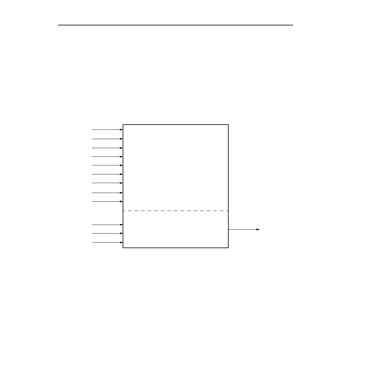
the FPGA portion of the ORT82G5. A block diagram of a memory block is shown in Figure 16. Each memory block
has a capacity of 4K word by 36 bit. It has one read port and one write port and four byte-write-enable (active-low)
signals. The read data from the memory block is registered so that it works as a pipelined synchronous memory
block. A block diagram of the memory block in shown below in Figure 16.The minimum timing specications are
shown in Figure 18.
2270(F)
Figure 16. Block Diagram of Memory Block
4K x 36
MEMORY BLOCK
(1 OF 2)
D_x[35:0]
CKW_x
CSWA_x
CSWB_x
AW_x[10:0]
BYTEWN_x[3]
BYTEWN_x[2]
BYTEWN_x[1]
BYTEWN_x[0]
BW[35,31:24]
BW[34,23:16]
BW[33,15:8]
BW[32,7:0]
CKR_x
CSR_x
AR_x[10:0]
Q_x[35:0]
WRITE PORTS
READ PORTS
相關PDF資料 |
PDF描述 |
|---|---|
| ORT82G5-2BM680 | FPGA, 1296 CLBS, 380000 GATES, PBGA680 |
| ORT82G5-3BM680 | FPGA, 1296 CLBS, 380000 GATES, PBGA680 |
| OS10040280G-012 | FIBER OPTIC RECEIVER, 1290-1600nm, PANEL MOUNT, FC/APC CONNECTOR |
| OT-WBSC-Y-A-10-X-9-M-3-05-FA | FIBER OPTIC SPLITTER/COUPLER, 1X2PORT, 10.0, PANEL MOUNT, FC/APC CONNECTOR |
| OT-WBSC-Y-A-50-13-9-F-1-05-FA | FIBER OPTIC SPLITTER/COUPLER, 1X2PORT, 50.0, PANEL MOUNT, FC/APC CONNECTOR |
相關代理商/技術參數(shù) |
參數(shù)描述 |
|---|---|
| ORT82G5-1BM680C | 功能描述:FPGA - 現(xiàn)場可編程門陣列 10368 LUT 372 I/O RoHS:否 制造商:Altera Corporation 系列:Cyclone V E 柵極數(shù)量: 邏輯塊數(shù)量:943 內(nèi)嵌式塊RAM - EBR:1956 kbit 輸入/輸出端數(shù)量:128 最大工作頻率:800 MHz 工作電源電壓:1.1 V 最大工作溫度:+ 70 C 安裝風格:SMD/SMT 封裝 / 箱體:FBGA-256 |
| ORT82G5-1BM680I | 功能描述:FPGA - 現(xiàn)場可編程門陣列 10368 LUT 372 I/O RoHS:否 制造商:Altera Corporation 系列:Cyclone V E 柵極數(shù)量: 邏輯塊數(shù)量:943 內(nèi)嵌式塊RAM - EBR:1956 kbit 輸入/輸出端數(shù)量:128 最大工作頻率:800 MHz 工作電源電壓:1.1 V 最大工作溫度:+ 70 C 安裝風格:SMD/SMT 封裝 / 箱體:FBGA-256 |
| ORT82G5-1F680C | 功能描述:FPGA - 現(xiàn)場可編程門陣列 ORCA FPSC 3.7GBITS/s BP XCVR 643K RoHS:否 制造商:Altera Corporation 系列:Cyclone V E 柵極數(shù)量: 邏輯塊數(shù)量:943 內(nèi)嵌式塊RAM - EBR:1956 kbit 輸入/輸出端數(shù)量:128 最大工作頻率:800 MHz 工作電源電壓:1.1 V 最大工作溫度:+ 70 C 安裝風格:SMD/SMT 封裝 / 箱體:FBGA-256 |
| ORT82G5-1F680I | 功能描述:FPGA - 現(xiàn)場可編程門陣列 ORCA FPSC 2.7Gbits/s BP XCVR 643K RoHS:否 制造商:Altera Corporation 系列:Cyclone V E 柵極數(shù)量: 邏輯塊數(shù)量:943 內(nèi)嵌式塊RAM - EBR:1956 kbit 輸入/輸出端數(shù)量:128 最大工作頻率:800 MHz 工作電源電壓:1.1 V 最大工作溫度:+ 70 C 安裝風格:SMD/SMT 封裝 / 箱體:FBGA-256 |
| ORT82G5-1FN680C | 功能描述:FPGA - 現(xiàn)場可編程門陣列 ORCA FPSC 1.5V 3.7 G b Bpln Xcvr 643K Gt RoHS:否 制造商:Altera Corporation 系列:Cyclone V E 柵極數(shù)量: 邏輯塊數(shù)量:943 內(nèi)嵌式塊RAM - EBR:1956 kbit 輸入/輸出端數(shù)量:128 最大工作頻率:800 MHz 工作電源電壓:1.1 V 最大工作溫度:+ 70 C 安裝風格:SMD/SMT 封裝 / 箱體:FBGA-256 |
發(fā)布緊急采購,3分鐘左右您將得到回復。