- 您現(xiàn)在的位置:買賣IC網(wǎng) > PDF目錄359236 > MTVX2602 (Zarlink Semiconductor Inc.) Managed 24 Port 10/100 Mbps Ethernet Switch PDF資料下載
參數(shù)資料
| 型號: | MTVX2602 |
| 廠商: | Zarlink Semiconductor Inc. |
| 英文描述: | Managed 24 Port 10/100 Mbps Ethernet Switch |
| 中文描述: | 管理的24端口10/100 Mbps以太網(wǎng)交換機 |
| 文件頁數(shù): | 55/147頁 |
| 文件大小: | 924K |
| 代理商: | MTVX2602 |
第1頁第2頁第3頁第4頁第5頁第6頁第7頁第8頁第9頁第10頁第11頁第12頁第13頁第14頁第15頁第16頁第17頁第18頁第19頁第20頁第21頁第22頁第23頁第24頁第25頁第26頁第27頁第28頁第29頁第30頁第31頁第32頁第33頁第34頁第35頁第36頁第37頁第38頁第39頁第40頁第41頁第42頁第43頁第44頁第45頁第46頁第47頁第48頁第49頁第50頁第51頁第52頁第53頁第54頁當前第55頁第56頁第57頁第58頁第59頁第60頁第61頁第62頁第63頁第64頁第65頁第66頁第67頁第68頁第69頁第70頁第71頁第72頁第73頁第74頁第75頁第76頁第77頁第78頁第79頁第80頁第81頁第82頁第83頁第84頁第85頁第86頁第87頁第88頁第89頁第90頁第91頁第92頁第93頁第94頁第95頁第96頁第97頁第98頁第99頁第100頁第101頁第102頁第103頁第104頁第105頁第106頁第107頁第108頁第109頁第110頁第111頁第112頁第113頁第114頁第115頁第116頁第117頁第118頁第119頁第120頁第121頁第122頁第123頁第124頁第125頁第126頁第127頁第128頁第129頁第130頁第131頁第132頁第133頁第134頁第135頁第136頁第137頁第138頁第139頁第140頁第141頁第142頁第143頁第144頁第145頁第146頁第147頁
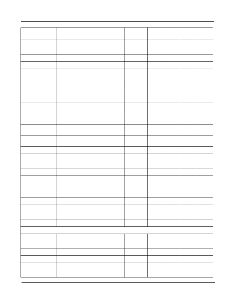
MVTX2602
Data Sheet
55
Zarlink Semiconductor Inc.
C7RS
Class 7 Reserve Size
516
R/W
0C0
000
QOSC"N"
QOS Control (N=0 - 39)
517- 53E
R/W
0C1-0D2
000
RDRC0
WRED Drop Rate Control 0
553
R/W
0FB
08F
RDRC1
WRED Drop Rate Control 1
554
R/W
0FC
088
USER_
PORT"N"_LOW
User Define Logical Port "N" Low (N=0-7)
580 + 2N
R/W
0D6-0DD
000
USER_
PORT"N"_HIGH
User Define Logical Port "N" High
581 + 2N
R/W
0DE-0E5
000
USER_ PORT1:0_
PRIORITY
User Define Logic Port 1 and 0 Priority
590
R/W
0E6
000
USER_ PORT3:2_
PRIORITY
User Define Logic Port 3 and 2 Priority
591
R/W
0E7
000
USER_ PORT5:4_
PRIORITY
User Define Logic Port 5 and 4 Priority
592
R/W
0E8
000
USER_ PORT7:6_
PRI ORITY
User Define Logic Port 7 and 6 Priority
593
R/W
0E9
000
USER_PORT_
ENABLE
User Define Logic Port Enable
594
R/W
0EA
000
WLPP10
Well known Logic Port Priority for 1 and 0
595
R/W
0EB
000
WLPP32
Well known Logic Port Priority for 3 and 2
596
R/W
0EC
000
WLPP54
Well known Logic Port Priority for 5 and 4
597
R/W
0ED
000
WLPP76
Well-known Logic Port Priority for 7 & 6
598
R/W
0EE
000
WLPE
Well known Logic Port Enable
599
R/W
0EF
000
RLOWL
User Define Range Low Bit7:0
59A
R/W
0F4
000
RLOWH
User Define Range Low Bit 15:8
59B
R/W
0F5
000
RHIGHL
User Define Range High Bit 7:0
59C
R/W
0D3
000
RHIGHH
User Define Range High Bit 15:8
59D
R/W
0D4
000
RPRIORITY
User Define Range Priority
59E
R/W
0D5
000
CPUQOSC1~3
Byte limit for TxQ on CPU port
5A0-5A2
R/W
NA
000
6. MISC Configuration Registers
MII_OP0
MII Register Option 0
600
R/W
0F0
000
MII_OP1
MII Register Option 1
601
R/W
0F1
000
FEN
Feature Registers
602
R/W
0F2
010
MIIC0
MII Command Register 0
603
R/W
N/A
000
MIIC1
MII Command Register 1
604
R/W
N/A
000
MIIC2
MII Command Register 2
605
R/W
N/A
000
Register
Description
CPU Addr
(Hex)
R/W
I2C Addr
(Hex)
Default
Notes
相關(guān)PDF資料 |
PDF描述 |
|---|---|
| MU456FC-RD | SUPER RED 0.56 FOUR DIGIT NUMERIC DISPLAYS |
| MU9C1480A-90DC | Content Addressable Memory |
| MU9C1480A-90DI | Content Addressable Memory |
| MU9C1480B-50TAC | Content Addressable Memory |
| MU9C1480B-70TAC | Content Addressable Memory |
相關(guān)代理商/技術(shù)參數(shù) |
參數(shù)描述 |
|---|---|
| MTW 106 D | 制造商:KNITTER-SWITCH 功能描述:TOGGLE SWITCH SPST ON-ON |
| MTW 106 E | 制造商:KNITTER-SWITCH 功能描述:SWITCH SPST ON-OFF-ON |
| MTW 106 G | 制造商:knitter-switch 功能描述: |
| MTW 206 N | 制造商:KNITTER-SWITCH 功能描述:TOGGLE SWITCH DPDT ON-ON |
| MTW 206 P | 制造商:KNITTER-SWITCH 功能描述:SWITCH DPDT ON-OFF-ON |
發(fā)布緊急采購,3分鐘左右您將得到回復(fù)。