- 您現(xiàn)在的位置:買賣IC網(wǎng) > PDF目錄371135 > MPC970 (Motorola, Inc.) LOW VOLTAGE PLL CLOCK DRIVER PDF資料下載
參數(shù)資料
| 型號: | MPC970 |
| 廠商: | Motorola, Inc. |
| 英文描述: | LOW VOLTAGE PLL CLOCK DRIVER |
| 中文描述: | 低壓PLL時(shí)鐘驅(qū)動器 |
| 文件頁數(shù): | 9/16頁 |
| 文件大小: | 213K |
| 代理商: | MPC970 |
MPC970
TIMING SOLUTIONS
BR1333 — Rev 6
9
MOTOROLA
output divide ratio. If the VCO_Sel pin is “LOW” the
multiplication factor will be reduced further by 2. (See “Using
the On–Board Crystal Oscillator” section of this datasheet.)
Using the External Feedback Feature of the MPC970/71
In applications where the relationship between the output
waveforms and the input waveforms are critical the external
feedback option will likely be used. Table 1 and Table 2 are
still appropriate for establishing the potential output
frequency relationships. The input reference frequency for
external feedback applications will be equal to the frequency
of the feedback signal. As a result the use of the external
feedback yields a number of potential input to output
frequency multiplication factors which are not available using
the internal feedback. Using the external feedback the device
can function as a zero delay buffer and could multiply the
input from 4 to as much as 48. In practice however the
multiplication factor is limited by the loop dynamics of the
PLL. The MPC970 PLL was optimized for an input reference
frequency or greater than 10MHz. Frequencies lower than
10MHz will tend to pass through the filter and add jitter to the
PLL. In addition the PLL was optimized for feedback divide
ratios of between 8 and 64. The user should avoid using the
device with feedback divide ratios outside of this range. For
the external feedback case the feedback divide ratio will
include the
÷
2 (if VCO_Sel is LOW) plus the output divider for
the feedback output. If, for instance the MPC970 is to be
used as a zero delay buffer the VCO_Sel pin should be pulled
LOW and all of the outputs should be set in a VCO/4 mode.
This would produce a feedback ratio of
÷
8. Several potential
configurations using the external feedback are pictured in
Figure 4 through Figure 7.
The external feedback option of the MPC970 is critical for
applications in which more than one clock driver need to be
synchronized. The external feedback option ensures that the
feed through delay is the same as the feedback delay. This
functionality removes propagation delay variation as a factor
in the determination of part to part skew. The low jitter PLL
used in the MPC970 has a near zero deadband phase
detector and very little part to part variability. The result is a
very low phase error variability in the product. When coupled
with the output to output skew the phase error variability
accounts for the part to part skew of the device. From the
specification table one sees that the worst case part to part
skew of the device is 800ps, assuming that there is zero
skew in the multiple reference inputs. For multiple MPC970
applications if the lowest generated output frequency is used
as the feedback signal the devices will be guaranteed to be
synchronized. For applications where the lowest frequency is
not used as the reference or where the internal feedback is
used there is no way to guarantee that the multiple devices
will be phase synchronized.
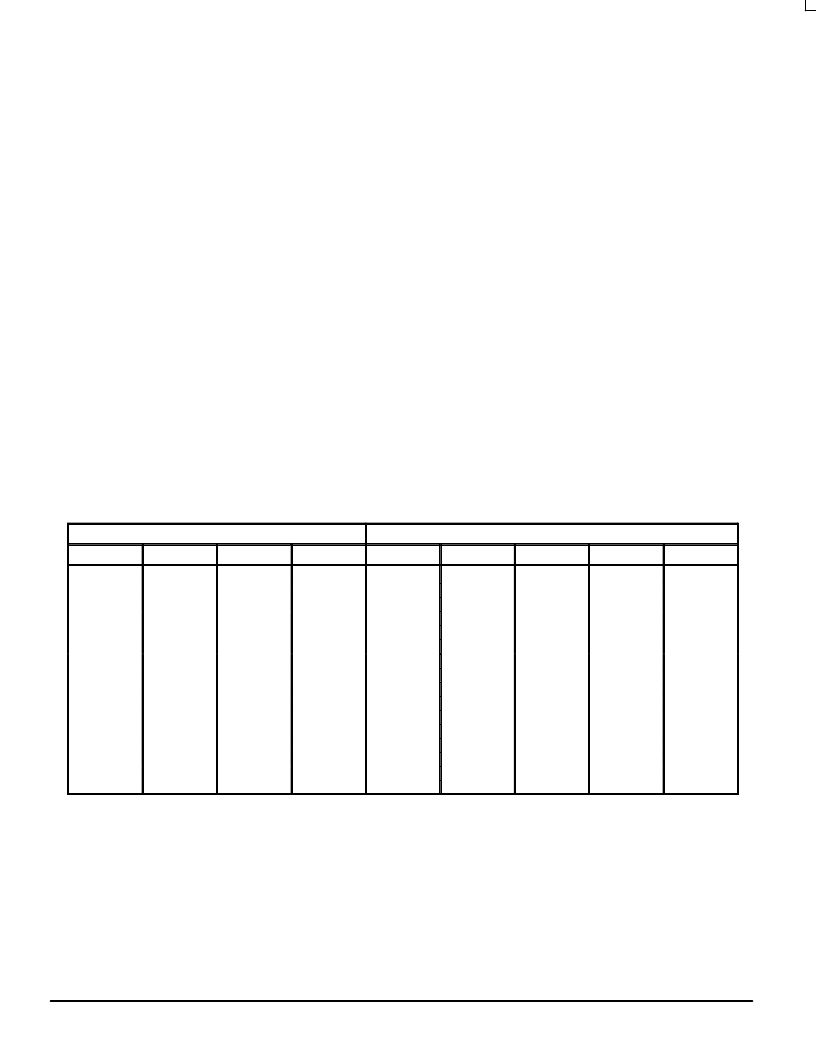
Table 1. Programmable Output Frequency Relationships
(MPC601_Clks = ‘HIGH’; VCO_Sel = ‘HIGH’)
INPUTS
OUTPUTS
PCI_Div1
PCI_Div0
BCLK_Div1
BCLK_Div0
2x_PCLK
PCLKEN
BCLKEN*
BCLK
PCI_CLK
0
0
0
0
0
0
0
0
1
1
1
1
1
1
1
1
0
0
0
0
1
1
1
1
0
0
0
0
1
1
1
1
0
0
1
1
0
0
1
1
0
0
1
1
0
0
1
1
0
1
0
1
0
1
0
1
0
1
0
1
0
1
0
1
VCO/2
VCO/2
VCO/2
VCO/2
VCO/2
VCO/2
VCO/2
VCO/2
VCO/2
VCO/2
VCO/2
VCO/2
VCO/2
VCO/2
VCO/2
VCO/2
VCO/4
VCO/4
VCO/4
VCO/4
VCO/4
VCO/4
VCO/4
VCO/4
VCO/4
VCO/4
VCO/4
VCO/4
VCO/4
VCO/4
VCO/4
VCO/4
VCO/4
VCO/8
VCO/12
VCO/16
VCO/4
VCO/8
VCO/12
VCO/16
VCO/4
VCO/8
VCO/12
VCO/16
VCO/4
VCO/8
VCO/12
VCO/16
VCO/4
VCO/8
VCO/12
VCO/16
VCO/4
VCO/8
VCO/12
VCO/16
VCO/4
VCO/8
VCO/12
VCO/16
VCO/4
VCO/8
VCO/12
VCO/16
VCO/4
VCO/8
VCO/12
VCO/16
VCO/8
VCO/16
VCO/24
VCO/32
VCO/12
VCO/24
VCO/36
VCO/48
VCO/4
VCO/4
VCO/4
VCO/4
* BCLK_En output is delayed relative to other outputs
相關(guān)PDF資料 |
PDF描述 |
|---|---|
| MPC972 | Low Voltage PLL Clock Driver(低壓PLL時(shí)鐘驅(qū)動器) |
| MPC973 | LOW VOLTAGE PLL CLOCK DRIVER |
| MPC974 | 3.3V PLL Clock Driver(3.3V PLL時(shí)鐘驅(qū)動器) |
| MPC9774 | 3.3V / 2,5V 1:14 LVCMOS PLL CLOCK GENERATOR |
| MPC980 | Dual 3.3V PLL Clock Generator(雙3.3V PLL時(shí)鐘發(fā)生器) |
相關(guān)代理商/技術(shù)參數(shù) |
參數(shù)描述 |
|---|---|
| MPC972 | 制造商:Motorola Inc 功能描述: |
| MPC972FA | 制造商:Freescale Semiconductor 功能描述: |
| MPC972H10 F44A WAF | 制造商:Motorola Inc 功能描述: |
| MPC973 | 制造商:MOTOROLA 制造商全稱:Motorola, Inc 功能描述:LOW VOLTAGE PLL CLOCK DRIVER |
| MPC974 | 制造商:MOTOROLA 制造商全稱:Motorola, Inc 功能描述:LOW VOLTAGE PLL CLOCK DRIVER |
發(fā)布緊急采購,3分鐘左右您將得到回復(fù)。