- 您現(xiàn)在的位置:買賣IC網(wǎng) > PDF目錄371135 > MPC970 (Motorola, Inc.) LOW VOLTAGE PLL CLOCK DRIVER PDF資料下載
參數(shù)資料
| 型號(hào): | MPC970 |
| 廠商: | Motorola, Inc. |
| 英文描述: | LOW VOLTAGE PLL CLOCK DRIVER |
| 中文描述: | 低壓PLL時(shí)鐘驅(qū)動(dòng)器 |
| 文件頁數(shù): | 12/16頁 |
| 文件大小: | 213K |
| 代理商: | MPC970 |
MPC970
MOTOROLA
TIMING SOLUTIONS
BR1333 — Rev 6
12
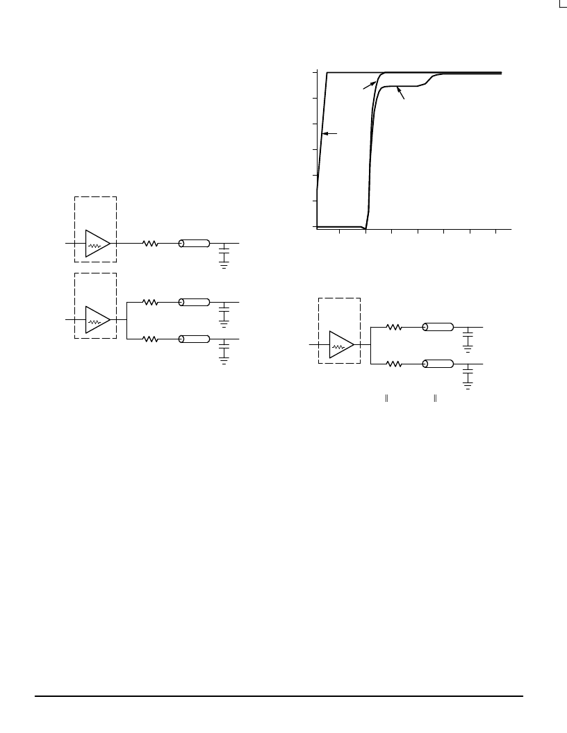
terminated transmission lines can be used. The parallel
technique terminates the signal at the end of the line with a
50
resistance to VCC/2. This technique draws a fairly high
level of DC current and thus only a single terminated line can
be driven by each output of the MPC970 clock driver. For the
series terminated case however there is no DC current draw,
thus the outputs can drive multiple series terminated lines.
Figure 9 illustrates an output driving a single series
terminated line vs two series terminated lines in parallel.
When taken to its extreme the fanout of the MPC970 clock
driver is effectively doubled due to its capability to drive
multiple lines.
Figure 9. Single versus Dual Transmission Lines
7
IN
MPC970
OUTPUT
BUFFER
RS = 43
ZO = 50
OutA
7
IN
MPC970
OUTPUT
BUFFER
RS = 43
ZO = 50
OutB0
RS = 43
ZO = 50
OutB1
The waveform plots of Figure 10 show the simulation
results of an output driving a single line vs two lines. In both
cases the drive capability of the MPC970 output buffers is
more than sufficient to drive 50
transmission lines on the
incident edge. Note from the delay measurements in the
simulations a delta of only 43ps exists between the two
differently loaded outputs. This suggests that the dual line
driving need not be used exclusively to maintain the tight
output–to–output skew of the MPC970. The output waveform
in Figure 10 shows a step in the waveform, this step is
caused by the impedance mismatch seen looking into the
driver. The parallel combination of the 43
series resistor
plus the output impedance does not match the parallel
combination of the line impedances. The voltage wave
launched down the two lines will equal:
VL = VS ( Zo / Rs + Ro +Zo) = 3.0 (25/53.5) = 1.40V
At the load end the voltage will double, due to the near
unity reflection coefficient, to 2.8V. It will then increment
towards the quiescent 3.0V in steps separated by one round
trip delay (in this case 4.0ns).
Since this step is well above the threshold region it will not
cause any false clock triggering, however designers may be
uncomfortable with unwanted reflections on the line. To
better match the impedances when driving multiple lines the
situation in Figure 11 should be used. In this case the series
terminating resistors are reduced such that when the parallel
combination is added to the output buffer impedance the line
impedance is perfectly matched.
Figure 10. Single versus Dual Waveforms
TIME (nS)
V
3.0
2.5
2.0
1.5
1.0
0.5
0
2
4
6
8
10
12
14
OutB
tD = 3.9386
OutA
tD = 3.8956
In
Figure 11. Optimized Dual Line Termination
7
MPC970
OUTPUT
BUFFER
RS = 36
ZO = 50
RS = 36
ZO = 50
7
+ 36
36
= 50
50
25
= 25
SPICE level output buffer models are available for
engineers who want to simulate their specific interconnect
schemes. In addition IV characteristics are in the process of
being generated to support the other board level simulators in
general use.
Using the Output Freeze Circuitry
With the recent advent of a “green” classification for
computers the desire for unique power management among
system designers is keen. The individual output enable
control of the MPC970 allows designers, under software
control, to implement unique power management schemes
into their designs. Although useful, individual output control
at the expense of one pin per output is too high, therefore a
simple serial interface was derived to economize on the
control pins.
The freeze control logic provides two mechanisms through
which the MPC970 clock outputs may be frozen (stopped in
the logic ‘0’ state):
The first freeze mechanism allows serial loading of the
13–bit Serial Input Register, this register contains one
programmable freeze enable bit for 13 of the 15 output
clocks. The BCLK0 and PCI_CLK0 outputs cannot be frozen
with the serial port, this avoids any potential lock up situation
相關(guān)PDF資料 |
PDF描述 |
|---|---|
| MPC972 | Low Voltage PLL Clock Driver(低壓PLL時(shí)鐘驅(qū)動(dòng)器) |
| MPC973 | LOW VOLTAGE PLL CLOCK DRIVER |
| MPC974 | 3.3V PLL Clock Driver(3.3V PLL時(shí)鐘驅(qū)動(dòng)器) |
| MPC9774 | 3.3V / 2,5V 1:14 LVCMOS PLL CLOCK GENERATOR |
| MPC980 | Dual 3.3V PLL Clock Generator(雙3.3V PLL時(shí)鐘發(fā)生器) |
相關(guān)代理商/技術(shù)參數(shù) |
參數(shù)描述 |
|---|---|
| MPC972 | 制造商:Motorola Inc 功能描述: |
| MPC972FA | 制造商:Freescale Semiconductor 功能描述: |
| MPC972H10 F44A WAF | 制造商:Motorola Inc 功能描述: |
| MPC973 | 制造商:MOTOROLA 制造商全稱:Motorola, Inc 功能描述:LOW VOLTAGE PLL CLOCK DRIVER |
| MPC974 | 制造商:MOTOROLA 制造商全稱:Motorola, Inc 功能描述:LOW VOLTAGE PLL CLOCK DRIVER |
發(fā)布緊急采購,3分鐘左右您將得到回復(fù)。