- 您現(xiàn)在的位置:買賣IC網(wǎng) > PDF目錄374310 > KAB03D100M-TNGP (SAMSUNG SEMICONDUCTOR CO. LTD.) Multi-Chip Package MEMORY PDF資料下載
參數(shù)資料
| 型號(hào): | KAB03D100M-TNGP |
| 廠商: | SAMSUNG SEMICONDUCTOR CO. LTD. |
| 英文描述: | Multi-Chip Package MEMORY |
| 中文描述: | 多芯片封裝存儲(chǔ)器 |
| 文件頁(yè)數(shù): | 70/72頁(yè) |
| 文件大?。?/td> | 1378K |
| 代理商: | KAB03D100M-TNGP |
第1頁(yè)第2頁(yè)第3頁(yè)第4頁(yè)第5頁(yè)第6頁(yè)第7頁(yè)第8頁(yè)第9頁(yè)第10頁(yè)第11頁(yè)第12頁(yè)第13頁(yè)第14頁(yè)第15頁(yè)第16頁(yè)第17頁(yè)第18頁(yè)第19頁(yè)第20頁(yè)第21頁(yè)第22頁(yè)第23頁(yè)第24頁(yè)第25頁(yè)第26頁(yè)第27頁(yè)第28頁(yè)第29頁(yè)第30頁(yè)第31頁(yè)第32頁(yè)第33頁(yè)第34頁(yè)第35頁(yè)第36頁(yè)第37頁(yè)第38頁(yè)第39頁(yè)第40頁(yè)第41頁(yè)第42頁(yè)第43頁(yè)第44頁(yè)第45頁(yè)第46頁(yè)第47頁(yè)第48頁(yè)第49頁(yè)第50頁(yè)第51頁(yè)第52頁(yè)第53頁(yè)第54頁(yè)第55頁(yè)第56頁(yè)第57頁(yè)第58頁(yè)第59頁(yè)第60頁(yè)第61頁(yè)第62頁(yè)第63頁(yè)第64頁(yè)第65頁(yè)第66頁(yè)第67頁(yè)第68頁(yè)第69頁(yè)當(dāng)前第70頁(yè)第71頁(yè)第72頁(yè)
KAB0xD100M - TxGP
TECHNICAL
NOTE
Revision 1.11
August 2003
- 70 -
MCP MEMORY
SEC Only
U
t
RAM USAGE AND TIMING
INTRODUCTION
U
t
RAM is based on single-transistor DRAM cells. As with any
other DRAM, the data in these cells must be periodically
refreshed to prevent data loss. What makes the U
t
RAM unique
is that it offers a true SRAM style interface that hides all refresh
operations from the memory controller.
START WITH A DRAM TECHNOLOGY
The key point of U
t
RAM is its high speed and low power. This
high speed comes from the use of many small blocks such as
32Kbits each to create U
t
RAM arrays. The small blocks have
short word lines thus with little capacitance eliminating a major
factor of operating current dissipation in conventional DRAM
blocks.
Each independent macro-cell on a U
t
RAM device consists of a
number of these blocks. Each chip has one or more macro.
The address decoding logic is also fast. U
t
RAM performs a
complete read operation in every tRC, but U
t
RAM needs power
up sequence like DRAM.
Power Up Sequence and Diagram
1. Apply power.
2. Maintain stable power for a minium 200
μ
s with CS
U
=high.
3. Issue read operation at least 2 times.
DESIGN ACHIEVES SRAM SPECIFIC
OPERATIONS
The U
t
RAM was designed to work just like an SRAM - without
any waits or other overhead for precharging or refreshing its
internal DRAM cells. SAMSUNG Electronics(SAMSUNG) hides
these operations inside with advanced design technology -
those are not to be seen from outside. Precharging takes place
during every access, overlapped between the end of the cycle
and the decoding portion of the next cycle.
Hiding refresh is more difficult. Every row in every block must
be refreshed at least once during the refresh interval to prevent
data loss. SAMSUNG provides an internal refresh controller for
devices. When all accesses within refresh interval are directed
to one macro-cell, as can happen in signal processing applica-
tions, a more sophisticated approach is required to hide
refresh. The pseudo SRAM is sometimes used on these appli-
cations, which requires a memory controller that can hold off
accesses when a refresh operation is needed. SAMSUNG’s
unique qualitative advantage over these parts(in addition to
quantitative improvements in access speed and power con-
sumption) is that the U
t
RAM never need to hold off accesses,
and indeed it has no hold off signal. The circuitry that gives
SAMSUNG this advantage is fairly simple but has not previ-
ously been disclosed.
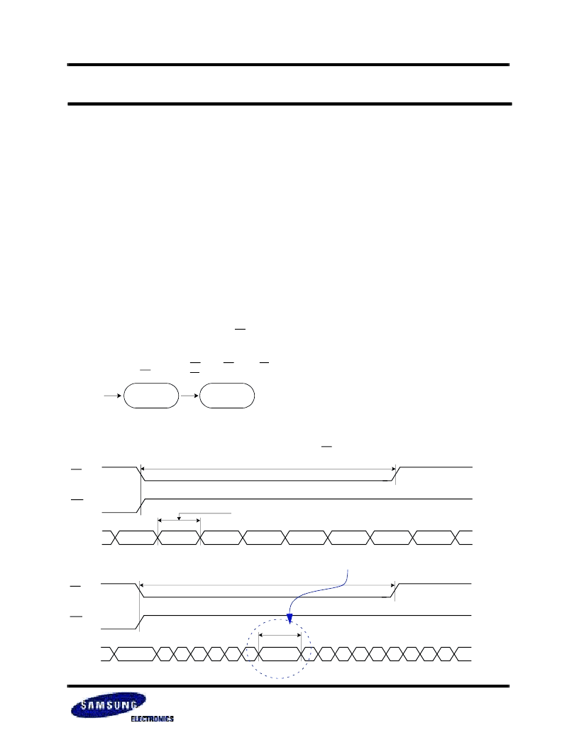
AVOID TIMING
Following figures show you an abnormal timing which is not
supported on U
t
RAM and its solution.
If your system has a timing which sustains invalid states over
4
μ
s at read mode like Figure 29, there are some guide lines for
proper operation of U
t
RAM.
When your system has multiple invalid address signals shorter
than tRC on the timing shown in Figure 1, U
t
RAM needs a nor-
mal read timing(tRC) during that cycle(Figure 30) or needs to
toggle CS
U
once to ’high’ for about ’tRC’(Figure 31).
CS
U
=V
IL
, UB or/and LB=V
IL
ZZ=V
IH
Read Operation(2 times)
Power On
Initial State
(Wait 200
μ
s)
Active
CS
U
=V
IH
CS
U
WE
Address
Less than tRC
Over 4
μ
s
CS
U
WE
Address
tRC
Over 4
μ
s
Figure 30.
Put on read operation every 4
μ
s
Figure 29.
相關(guān)PDF資料 |
PDF描述 |
|---|---|
| KAB04D100M-TLGP | Multi-Chip Package MEMORY |
| KAB04D100M-TNGP | Multi-Chip Package MEMORY |
| KAB01D100M | Tantalum Conformal-Coated Capacitor; Capacitance: 22uF; Voltage: 10V; Packaging: Tape & Reel |
| KAB02D100M-TLGP | Tantalum Conformal-Coated Capacitor; Capacitance: 22uF; Voltage: 10V; Packaging: Tape & Reel |
| KAB01D100M-TNGP | CONNECTOR ACCESSORY |
相關(guān)代理商/技術(shù)參數(shù) |
參數(shù)描述 |
|---|---|
| KAB04D100M-TLGP | 制造商:SAMSUNG 制造商全稱:Samsung semiconductor 功能描述:Multi-Chip Package MEMORY |
| KAB04D100M-TNGP | 制造商:SAMSUNG 制造商全稱:Samsung semiconductor 功能描述:Multi-Chip Package MEMORY |
| KAB-1 | 功能描述:保險(xiǎn)絲 TRON RECTIFIER FUSE RoHS:否 制造商:Littelfuse 產(chǎn)品:Surface Mount Fuses 電流額定值:0.5 A 電壓額定值:600 V 保險(xiǎn)絲類型:Fast Acting 保險(xiǎn)絲大小/組:Nano 尺寸:12.1 mm L x 4.5 mm W 安裝風(fēng)格: 端接類型:SMD/SMT 系列:485 |
| KAB-1/2 | 制造商:COOPER BUSSMANN 功能描述:TRON RECTIFIER FUSE |
| KAB-10 | 功能描述:保險(xiǎn)絲 10A RoHS:否 制造商:Littelfuse 產(chǎn)品:Surface Mount Fuses 電流額定值:0.5 A 電壓額定值:600 V 保險(xiǎn)絲類型:Fast Acting 保險(xiǎn)絲大小/組:Nano 尺寸:12.1 mm L x 4.5 mm W 安裝風(fēng)格: 端接類型:SMD/SMT 系列:485 |
發(fā)布緊急采購(gòu),3分鐘左右您將得到回復(fù)。