- 您現(xiàn)在的位置:買賣IC網(wǎng) > PDF目錄385399 > HT46C24 (Holtek Semiconductor Inc.) A/D Type 8-Bit MCU PDF資料下載
參數(shù)資料
| 型號: | HT46C24 |
| 廠商: | Holtek Semiconductor Inc. |
| 英文描述: | A/D Type 8-Bit MCU |
| 中文描述: | 的A / D型8位微控制器 |
| 文件頁數(shù): | 17/49頁 |
| 文件大小: | 393K |
| 代理商: | HT46C24 |
第1頁第2頁第3頁第4頁第5頁第6頁第7頁第8頁第9頁第10頁第11頁第12頁第13頁第14頁第15頁第16頁當前第17頁第18頁第19頁第20頁第21頁第22頁第23頁第24頁第25頁第26頁第27頁第28頁第29頁第30頁第31頁第32頁第33頁第34頁第35頁第36頁第37頁第38頁第39頁第40頁第41頁第42頁第43頁第44頁第45頁第46頁第47頁第48頁第49頁

HT46R24/HT46C24
Rev. 1.50
17
May 3, 2004
Some instructions first input data and then follow the
output operations. For example,
SET [m].i ,
CLR
[m].i , CPL [m] , CPLA [m] read the entire port states
into the CPU, execute the defined operations
(bit-operation), and then write the results back to the
latches or the accumulator.
Each line of port A has the capability of waking-up the
device. Each I/O port has a pull-high option. Once the
pull-high option is selected, the I/O port has a pull-high
resistor, otherwise, there s none. Take note that a
non-pull-high I/O port operating in input mode will cause
a floating state.
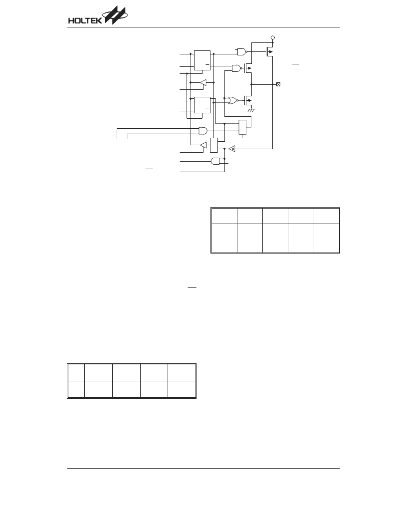
The PA3 and PA5 are pin-shared with the PFD and INT
pins respectively. If the PFD option is selected, the out-
put signal in output mode of PA3 will be the PFD signal
generated by timer/event counter overflow signal. The
input mode always remain in its original functions. Once
the PFD option is selected, the PFD output signal is con-
trolled by PA3 data register only. Writing 1 to PA3 data
registerwillenablethePFDoutputfunctionandwriting0
will force the PA3 to remain at 0 . The I/O functions of
PA3 are shown below.
I/O
Mode
I/P
(Normal)
O/P
(Normal)
I/P
(PFD)
O/P
(PFD)
PA3
Logical
Input
Logical
Output
Logical
Input
PFD
(Timer on)
Note:
The PFD frequency is the timer/event counter
overflow frequency divided by 2.
The PB can also be used as A/D converter inputs. The
A/D function will be described later. There is a PWM
function shared with PD0/PD1/PD2/PD3. If the PWM
function is enabled, the PWM0/PWM1/PWM2/PWM3
signal will appear on PD0/PD1/PD2/PD3 (if PD0/PD1/
PD2/PD3 is operating in output mode). The I/O func-
tions of PD0/PD1/PD2/PD3 are as shown.
I/O
Mode
I/P
(Normal)
O/P
(Normal)
I/P
(PWM)
O/P
(PWM)
PD0
PD1
PD2
PD3
Logical
Input
Logical
Output
Logical
Input
PWM0
PWM1
PWM2
PWM3
It is recommended that unused or not bonded out I/O
linesshouldbesetasoutputpinsbysoftwareinstruction
to avoid consuming power under input floating state.
PWM
The microcontroller provides 4 channels (6+2)/(7+1)
(depends on options) bits PWM output shared with
PD0/PD1/PD2/PD3.ThePWMchannelshavetheirdata
registers denoted as PWM0 (1AH), PWM1 (1BH),
PWM2 (1CH) and PWM3 (1DH). The frequency source
of the PWM counter comes from f
SYS
. The PWM regis-
ters are four 8-bit registers. The waveforms of PWM out-
puts are as shown. Once the PD0/PD1/PD2/PD3 are
selected as the PWM outputs and the output function of
PD0/PD1/PD2/PD3 are enabled (PDC.0/PDC.1/
PDC.2/PDC.3 = 0 ), writing 1 to PD0/PD1/PD2/PD3
data register will enable the PWM output function and
writing 0 will force the PD0/PD1/PD2/PD3 to stay at
0 .
A(6+2) bits mode PWM cycle is divided into four modu-
lation cycles (modulation cycle 0~modulation cycle 3).
Each modulation cycle has 64 PWM input clock period.
In a (6+2) bit PWM function, the contents of the PWM
register is divided into two groups. Group 1 of the PWM
register is denoted by DC which is the value of
PWM.7~PWM.2.
9
+
*
)
( /
)
0 ;
( /
1
* $
*
6 *
.
* )
>
4
9
*
. ;
! *
*
F
F
F
. * 2
* 2
)
*
. *
#
*
! *
. *
)
*
*
* 2
( /
0 '
+
-
6 '
7 '
1 '
"
2 ( '
( /
2 1 '
1
( /
1
( '
)
(
'
)
'
)
0 '
)
0
- /
1
+ ( /
+ 1
F
* * * * * * * * * * * * * * * * * G
0 : *
+
H * * *
* G
( :
)
( H
* G
:
)
H
* G
:
)
H
* G
0 :
)
0 H
Input/Output Ports
相關PDF資料 |
PDF描述 |
|---|---|
| HT46R24 | A/D Type 8-Bit MCU |
| HT46C46 | Cost-Effective A/D Type 8-Bit MCU |
| HT46C47 | Cost-Effective A/D Type 8-Bit MCU |
| HT46R46 | Cost-Effective A/D Type 8-Bit MCU |
| HT46C62 | A/D with LCD Type 8-Bit MCU |
相關代理商/技術參數(shù) |
參數(shù)描述 |
|---|---|
| HT46C46 | 制造商:HOLTEK 制造商全稱:Holtek Semiconductor Inc 功能描述:Cost-Effective A/D Type 8-Bit MCU |
| HT46C46E | 制造商:HOLTEK 制造商全稱:Holtek Semiconductor Inc 功能描述:Cost-Effective A/D Type 8-Bit MCU |
| HT46C47 | 制造商:HOLTEK 制造商全稱:Holtek Semiconductor Inc 功能描述:Cost-Effective A/D Type 8-Bit MCU |
| HT46C47E | 制造商:HOLTEK 制造商全稱:Holtek Semiconductor Inc 功能描述:Cost-Effective A/D Type 8-Bit MCU |
| HT46C48A | 制造商:HOLTEK 制造商全稱:Holtek Semiconductor Inc 功能描述:Cost-Effective A/D Type 8-Bit MCU |
發(fā)布緊急采購,3分鐘左右您將得到回復。