- 您現(xiàn)在的位置:買賣IC網(wǎng) > PDF目錄376976 > DS3174N Single/Dual/Triple/Quad DS3/E3 Single-Chip Transceivers PDF資料下載
參數(shù)資料
| 型號: | DS3174N |
| 英文描述: | Single/Dual/Triple/Quad DS3/E3 Single-Chip Transceivers |
| 中文描述: | 單/雙/三/四DS3/E3單芯片收發(fā)器 |
| 文件頁數(shù): | 58/232頁 |
| 文件大小: | 2133K |
| 代理商: | DS3174N |
第1頁第2頁第3頁第4頁第5頁第6頁第7頁第8頁第9頁第10頁第11頁第12頁第13頁第14頁第15頁第16頁第17頁第18頁第19頁第20頁第21頁第22頁第23頁第24頁第25頁第26頁第27頁第28頁第29頁第30頁第31頁第32頁第33頁第34頁第35頁第36頁第37頁第38頁第39頁第40頁第41頁第42頁第43頁第44頁第45頁第46頁第47頁第48頁第49頁第50頁第51頁第52頁第53頁第54頁第55頁第56頁第57頁當(dāng)前第58頁第59頁第60頁第61頁第62頁第63頁第64頁第65頁第66頁第67頁第68頁第69頁第70頁第71頁第72頁第73頁第74頁第75頁第76頁第77頁第78頁第79頁第80頁第81頁第82頁第83頁第84頁第85頁第86頁第87頁第88頁第89頁第90頁第91頁第92頁第93頁第94頁第95頁第96頁第97頁第98頁第99頁第100頁第101頁第102頁第103頁第104頁第105頁第106頁第107頁第108頁第109頁第110頁第111頁第112頁第113頁第114頁第115頁第116頁第117頁第118頁第119頁第120頁第121頁第122頁第123頁第124頁第125頁第126頁第127頁第128頁第129頁第130頁第131頁第132頁第133頁第134頁第135頁第136頁第137頁第138頁第139頁第140頁第141頁第142頁第143頁第144頁第145頁第146頁第147頁第148頁第149頁第150頁第151頁第152頁第153頁第154頁第155頁第156頁第157頁第158頁第159頁第160頁第161頁第162頁第163頁第164頁第165頁第166頁第167頁第168頁第169頁第170頁第171頁第172頁第173頁第174頁第175頁第176頁第177頁第178頁第179頁第180頁第181頁第182頁第183頁第184頁第185頁第186頁第187頁第188頁第189頁第190頁第191頁第192頁第193頁第194頁第195頁第196頁第197頁第198頁第199頁第200頁第201頁第202頁第203頁第204頁第205頁第206頁第207頁第208頁第209頁第210頁第211頁第212頁第213頁第214頁第215頁第216頁第217頁第218頁第219頁第220頁第221頁第222頁第223頁第224頁第225頁第226頁第227頁第228頁第229頁第230頁第231頁第232頁
DS3171/DS3172/DS3173/DS3174
58 of 231
Table 18-1., will not be valid. There are some combinations of TFTS=1 and other modes in which there is no input
clock pin available for external timing since the clock source is derived internally from the RX LIU or the CLAD.
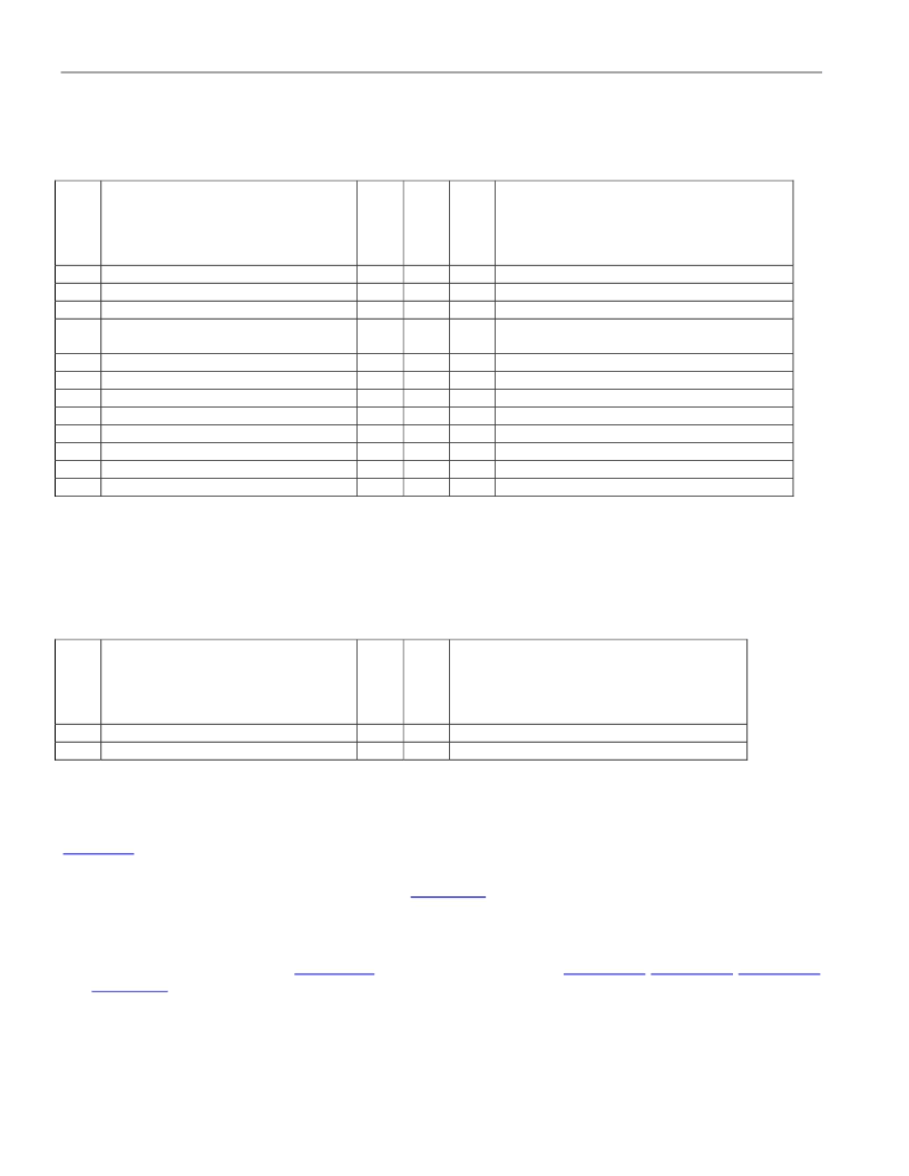
Table 10-7. Transmit Framer Pin Signal Timing Source Select
L
LBM[2:0]
L
C
T
Valid Timing to These Clock Pins
1
1
1
0
XXX
XXX
XXX
X
0
1
0
X
X
X
X
0
1
1
0
TCLKOn, TLCLKn, RCLKOn
RLCLKn
No valid timing to any input clock pin
TCLKOn, TLCLKn, RCLKOn
PLB (011) or DLB (100) or
ALB(001)
PLB (011) or DLB (100)
DLB&LLB (110)
LLB (010)
not LLB, DLB or PLB (00X)
not PLB (011)
not PLB (011)
PLB (011)
PLB (011)
0
0
0
0
0
0
0
0
1
X
X
X
X
X
0
1
X
X
X
X
0
1
X
X
0
0
0
0
1
1
1
1
TCLKOn, TLCLKn, RCLKOn
TCLKOn, RCLKOn
TCLKOn
TCLKOn, TLCLKn
No valid timing to any input clock pin
TCLKIn
RLCLKn
No valid timing to any input clock pin
10.2.3.3 Receive Line Interface Pin Timing Source Selection
(RPOSn/RDATn, RNEGn/RLCVn)
The receive line interface signal pin group must clocked in with the RLCLK clock input pin. When the LIU is
enabled, the receive line interface pins are not used so there is no valid clock reference.
Table 10-8. Receive Line Interface Pin Signal Timing Source Select
L
LBM[2:0]
L
C
Valid Timing to These Clock Pins
X
X
XXX
XXX
0
1
X
X
RLCLKn
No valid timing to any clock pin
10.2.3.4 Receiver Framer Pin Timing Source Selection
(RSERn, RSOFOn/RDENn)
The receive framer signal pin group has the same functional timing clock source as the RCLKOn pin described in
Table 10-5
.
Other clock pins can be used for the external timing. The RCLKOn receive clock output pin is always a valid output
clock for external logic to use for these signals when
PORT.CR3
.RFTS=0.
The receive framer timing select bit (RFTS) is used to select input or output clock pin timing. When RFTS=0, output
clock timing is selected. When RFTS=1, input clock timing is selected. If RFTS is set for input clock timing and an
output clock pin is used, or If RFTS is set for output clock timing and an input clock pin is used, then the setup, hold
and delay timings, as specified in
The generic
timing definitions shown in
Figure 18-1,
Figure 18-2,
Figure 18-3,
and
Figure 18-6
apply to this interface.
Table 18-1. will not be valid. There are some combinations of RFTS=1 and other modes in which there is no input
clock pin available for external timing since the clock source is derived internally from the RX LIU or the CLAD.
相關(guān)PDF資料 |
PDF描述 |
|---|---|
| DS318PIN | Industrial Control IC |
| DS319 | Two-Way Power Divider 10500 MHz |
| DS109333 | Two-Way Power Divider 10500 MHz |
| DS322 | 32 Megabit (4 M x 8-Bit/2 M x 16-Bit) CMOS 1.8 Volt-only, Simultaneous Operation Flash Memory |
| DS323 | 32 Megabit (4 M x 8-Bit/2 M x 16-Bit) CMOS 1.8 Volt-only, Simultaneous Operation Flash Memory |
相關(guān)代理商/技術(shù)參數(shù) |
參數(shù)描述 |
|---|---|
| DS3174N+ | 功能描述:網(wǎng)絡(luò)控制器與處理器 IC Quad DS3/E3 Single Chip Transceiver RoHS:否 制造商:Micrel 產(chǎn)品:Controller Area Network (CAN) 收發(fā)器數(shù)量: 數(shù)據(jù)速率: 電源電流(最大值):595 mA 最大工作溫度:+ 85 C 安裝風(fēng)格:SMD/SMT 封裝 / 箱體:PBGA-400 封裝:Tray |
| DS3177+ | 制造商:Maxim Integrated Products 功能描述:IC TXRX DS3/E3 CSBGA |
| DS3177N+ | 制造商:Maxim Integrated Products 功能描述:DS3/E3 SINGLE-CHIP TRANSCEIVER - Rail/Tube 制造商:Maxim Integrated Products 功能描述:IC TXRX DS3/E3 CSBGA |
| DS3177N+T | 制造商:Maxim Integrated Products 功能描述:DS3/E3 SINGLE-CHIP TRANSCEIVER - Tape and Reel |
| DS-318 | 制造商:MA-COM 制造商全稱:M/A-COM Technology Solutions, Inc. 功能描述:Plug-In Two-Way Power Divider, 5 - 500 MHz |
發(fā)布緊急采購,3分鐘左右您將得到回復(fù)。