- 您現在的位置:買賣IC網 > PDF目錄376976 > DS3174N Single/Dual/Triple/Quad DS3/E3 Single-Chip Transceivers PDF資料下載
參數資料
| 型號: | DS3174N |
| 英文描述: | Single/Dual/Triple/Quad DS3/E3 Single-Chip Transceivers |
| 中文描述: | 單/雙/三/四DS3/E3單芯片收發(fā)器 |
| 文件頁數: | 230/232頁 |
| 文件大小: | 2133K |
| 代理商: | DS3174N |
第1頁第2頁第3頁第4頁第5頁第6頁第7頁第8頁第9頁第10頁第11頁第12頁第13頁第14頁第15頁第16頁第17頁第18頁第19頁第20頁第21頁第22頁第23頁第24頁第25頁第26頁第27頁第28頁第29頁第30頁第31頁第32頁第33頁第34頁第35頁第36頁第37頁第38頁第39頁第40頁第41頁第42頁第43頁第44頁第45頁第46頁第47頁第48頁第49頁第50頁第51頁第52頁第53頁第54頁第55頁第56頁第57頁第58頁第59頁第60頁第61頁第62頁第63頁第64頁第65頁第66頁第67頁第68頁第69頁第70頁第71頁第72頁第73頁第74頁第75頁第76頁第77頁第78頁第79頁第80頁第81頁第82頁第83頁第84頁第85頁第86頁第87頁第88頁第89頁第90頁第91頁第92頁第93頁第94頁第95頁第96頁第97頁第98頁第99頁第100頁第101頁第102頁第103頁第104頁第105頁第106頁第107頁第108頁第109頁第110頁第111頁第112頁第113頁第114頁第115頁第116頁第117頁第118頁第119頁第120頁第121頁第122頁第123頁第124頁第125頁第126頁第127頁第128頁第129頁第130頁第131頁第132頁第133頁第134頁第135頁第136頁第137頁第138頁第139頁第140頁第141頁第142頁第143頁第144頁第145頁第146頁第147頁第148頁第149頁第150頁第151頁第152頁第153頁第154頁第155頁第156頁第157頁第158頁第159頁第160頁第161頁第162頁第163頁第164頁第165頁第166頁第167頁第168頁第169頁第170頁第171頁第172頁第173頁第174頁第175頁第176頁第177頁第178頁第179頁第180頁第181頁第182頁第183頁第184頁第185頁第186頁第187頁第188頁第189頁第190頁第191頁第192頁第193頁第194頁第195頁第196頁第197頁第198頁第199頁第200頁第201頁第202頁第203頁第204頁第205頁第206頁第207頁第208頁第209頁第210頁第211頁第212頁第213頁第214頁第215頁第216頁第217頁第218頁第219頁第220頁第221頁第222頁第223頁第224頁第225頁第226頁第227頁第228頁第229頁當前第230頁第231頁第232頁
DS3171/DS3172/DS3173/DS3174
230 of 232
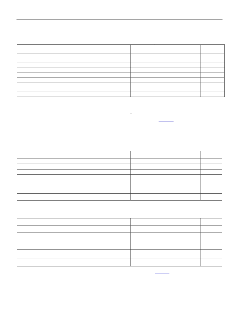
Table 18-10. Receiver Input Characteristics—E3 Mode
(V
DD
= 3.3V 5%, T
A
= -40°C to +85°C.)
PARAMETER
MIN
TYP
MAX
UNITS
Receive Sensitivity (Length of Cable)
Signal-to-Noise Ratio, Interfering Signal Test (Notes 2, 3)
Input Pulse Amplitude, RMON = 0 (Notes 2, 3)
Input Pulse Amplitude, RMON = 1 (Notes 2, 3)
Analog LOS Declare, RMON = 0 (Note 4)
Analog LOS Clear, RMON = 0 (Note 4)
Analog LOS Declare, RMON = 1 (Note 4)
Analog LOS Clear, RMON = 1 (Note 4)
Intrinsic Jitter Generation (Note 2)
900
-16
-29
1200
12
-24
-17
0.03
ft
1300
260
-28
-38
mVpk
mVpk
dB
dB
dB
dB
UI
P-P
Note 1:
An interfering signal (2
15
– 1 PRBS for DS3, 2
23
– 1 PRBS for E3, B3ZS/HDB3 encoded, compliant waveshape, nominal bit rate) is
added to the wanted signal. The combined signal is passed through 0 to 900ft of coaxial cable and presented to the LIU. This spec
indicates the lowest signal-to-noise ratio that results in a bit error ratio <10
.
Note 2:
Not tested during production test.
Note 3:
Measured on the line side (i.e., the BNC connector side) of the 1:2 receive transformer (
Figure 1-1
). During measurement, incoming
data traffic is unframed 2
– 1 PRBS for DS3 and unframed 2
– 1 PRBS for E3.
Note 4:
With respect to nominal 800mVpk signal for DS3 and nominal 1000mVpk signal for E3.
Table 18-11. Transmitter Output Characteristics—DS3 Modes
(V
DD
= 3.3V 5%, T
A
= -40°C to +85°C.)
PARAMETER
MIN
700
520
0.9
TYP
800
700
MAX
900
800
1.1
UNITS
mVpk
mVpk
DS3 Output Pulse Amplitude, TLBO = 0 (Note 5)
DS3 Output Pulse Amplitude, TLBO = 1 (Note 5)
Ratio of Positive and Negative Pulse-Peak Amplitudes
DS3 Unframed All-Ones Power Level at 22.368MHz, 3kHz
Bandwidth
DS3 Unframed All-Ones Power Level at 44.736MHz vs.
Power Level at 22.368MHz, 3kHz Bandwidth
Intrinsic Jitter Generation (Note 6)
-1.8
+5.7
dBm
-20
dB
0.02
0.05
UI
P-P
Table 18-12. Transmitter Output Characteristics—E3 Mode
(V
DD
= 3.3V 5%, T
A
= -40°C to +85°C.)
PARAMETER
MIN
TYP
MAX
UNITS
Output Pulse Amplitude (Note 5)
900
1000
1100
mVpk
Pulse Width
Ratio of Positive and Negative Pulse Amplitudes (at Centers
of Pulses)
Ratio of Positive and Negative Pulse Widths (at Nominal Half
Amplitude)
Intrinsic Jitter Generation (Note 6)
14.55
ns
0.95
1.05
0.95
1.05
0.02
0.05
UI
P-P
Note 5:
Measured on the line side (i.e., the BNC connector side) of the 2:1 transmit transformer (
Figure 1-1
).
Note 6:
Measured with jitter-free clock applied to TCLK and a bandpass jitter filter with 10Hz and 800kHz cutoff frequencies. Not tested during
production test.
相關PDF資料 |
PDF描述 |
|---|---|
| DS318PIN | Industrial Control IC |
| DS319 | Two-Way Power Divider 10500 MHz |
| DS109333 | Two-Way Power Divider 10500 MHz |
| DS322 | 32 Megabit (4 M x 8-Bit/2 M x 16-Bit) CMOS 1.8 Volt-only, Simultaneous Operation Flash Memory |
| DS323 | 32 Megabit (4 M x 8-Bit/2 M x 16-Bit) CMOS 1.8 Volt-only, Simultaneous Operation Flash Memory |
相關代理商/技術參數 |
參數描述 |
|---|---|
| DS3174N+ | 功能描述:網絡控制器與處理器 IC Quad DS3/E3 Single Chip Transceiver RoHS:否 制造商:Micrel 產品:Controller Area Network (CAN) 收發(fā)器數量: 數據速率: 電源電流(最大值):595 mA 最大工作溫度:+ 85 C 安裝風格:SMD/SMT 封裝 / 箱體:PBGA-400 封裝:Tray |
| DS3177+ | 制造商:Maxim Integrated Products 功能描述:IC TXRX DS3/E3 CSBGA |
| DS3177N+ | 制造商:Maxim Integrated Products 功能描述:DS3/E3 SINGLE-CHIP TRANSCEIVER - Rail/Tube 制造商:Maxim Integrated Products 功能描述:IC TXRX DS3/E3 CSBGA |
| DS3177N+T | 制造商:Maxim Integrated Products 功能描述:DS3/E3 SINGLE-CHIP TRANSCEIVER - Tape and Reel |
| DS-318 | 制造商:MA-COM 制造商全稱:M/A-COM Technology Solutions, Inc. 功能描述:Plug-In Two-Way Power Divider, 5 - 500 MHz |
發(fā)布緊急采購,3分鐘左右您將得到回復。