- 您現(xiàn)在的位置:買賣IC網(wǎng) > PDF目錄374047 > ADV7312KST (ANALOG DEVICES INC) Multiformat 11-Bit HDTV Video Encoder PDF資料下載
參數(shù)資料
| 型號: | ADV7312KST |
| 廠商: | ANALOG DEVICES INC |
| 元件分類: | 顏色信號轉(zhuǎn)換 |
| 英文描述: | Multiformat 11-Bit HDTV Video Encoder |
| 中文描述: | COLOR SIGNAL ENCODER, PQFP64 |
| 封裝: | MS-026BCD, LQFP-64 |
| 文件頁數(shù): | 38/84頁 |
| 文件大小: | 975K |
| 代理商: | ADV7312KST |
第1頁第2頁第3頁第4頁第5頁第6頁第7頁第8頁第9頁第10頁第11頁第12頁第13頁第14頁第15頁第16頁第17頁第18頁第19頁第20頁第21頁第22頁第23頁第24頁第25頁第26頁第27頁第28頁第29頁第30頁第31頁第32頁第33頁第34頁第35頁第36頁第37頁當前第38頁第39頁第40頁第41頁第42頁第43頁第44頁第45頁第46頁第47頁第48頁第49頁第50頁第51頁第52頁第53頁第54頁第55頁第56頁第57頁第58頁第59頁第60頁第61頁第62頁第63頁第64頁第65頁第66頁第67頁第68頁第69頁第70頁第71頁第72頁第73頁第74頁第75頁第76頁第77頁第78頁第79頁第80頁第81頁第82頁第83頁第84頁
REV. 0
–38–
ADV7312
Vertical Blanking Interval
The ADV7312 accept input data that contains VBI data
[CGMS, WSS, VITS, and so on] in SD and HD modes.
For SMPTE 293M [525p] standards, VBI data can be inserted
on Lines 13 to 42 of each frame, or on Lines 6 to 43 for the
ITU-R BT.1358 [625p] standard.
For SD NTSC this data can be present on Lines 10 to 20, and
in PAL on Lines 7 to 22.
If VBI is disabled [Address 11h, Bit 4 for HD; Address 43h,
Bit 4 for SD], VBI data is not present at the output and the
entire VBI is blanked. These control bits are valid in all master
and slave modes.
In Slave Mode 0, if VBI is enabled, the blanking bit in the
EAV/SAV code is overwritten, and it is possible to use VBI in
this timing mode as well.
In Slave Mode 1 or 2, the
BLANK
control bit must be set to
enabled [Address 4Ah, Bit 3] to allow VBI data to pass through
the ADV7312. Otherwise, the ADV7312 automatically blanks
the VBI to standard.
If CGMS is enabled and VBI is disabled, the CGMS data will
nevertheless be available at the output.
Subcarrier Frequency Registers
[Subaddress 4Ch–4Fh]
Four 8-bit registers are used to set up the subcarrier frequency.
The value of these registers is calculated using the equation
Subcarrier Frequency Register
Number of subcarrier frequencyvaluesinonevideoline
Numberof 27 MHz clkcyclesinonevideoline
=
2
23
*
*
Rounded to the nearest integer
For example, in NTSC mode,
Subcarrier FrequencyValue
=
×
=
227.5
1716
2
569408542
23
Subcarrier Register Value = 21F07C1Eh
SD F
SC
Register 0: 1Eh
SD F
SC
Register 1: 7Ch
SD F
SC
Register 2: F0h
SD F
SC
Register 3: 21h
Refer to the MPU Port Description section for more details on
how to access the subcarrier frequency registers.
Square Pixel Timing
[Register 42h, Bit 4]
In square pixel mode, the following timing diagrams apply.
Y
C
r
Y
F
F
0
0
0
0
X
Y
8
0
1
0
8
0
1
0
F
F
0
0
F
F
A
B
A
B
A
B
8
0
1
0
8
0
1
0
F
F
0
0
0
0
X
Y
C
b
YC
r
C
b
Y
C
b
Y
C
r
EAV CODE
SAV CODE
ANCILLARY DATA
(HANC)
272 CLOCK
4 CLOCK
4 CLOCK
1280 CLOCK
4 CLOCK
4 CLOCK
344 CLOCK
1536 CLOCK
END OF ACTIVE
VIDEO LINE
START OF ACTIVE
VIDEO LINE
ANALOG
VIDEO
INPUT PIXELS
NTSC/PAL M SYSTEM
(525 LINES/60Hz)
PAL SYSTEM
(625 LINES/50Hz)
Y
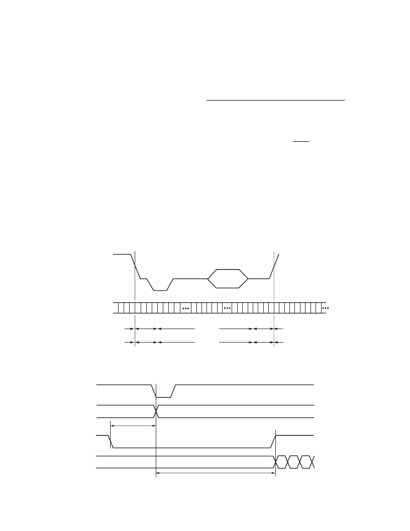
Figure 33. EAV/SAV Embedded Timing
FIELD
PIXEL
DATA
PAL = 44 CLOCK CYCLES
NTSC = 44 CLOCK CYCLES
PAL = 136 CLOCK CYCLES
NTSC = 208 CLOCK CYCLES
Cb
Y
Cr
Y
HSYNC
BLANK
Figure 34. Active Pixel Timing
相關(guān)PDF資料 |
PDF描述 |
|---|---|
| ADV7320KSTZ | Multiformat 216 MHz Video Encoder with Six NSV 12-Bit DACs |
| ADV7320 | Multiformat 216 MHz Video Encoder with Six NSV 12-Bit DACs |
| ADV7321 | Multiformat 216 MHz Video Encoder with Six NSV 12-Bit DACs |
| ADV7321KSTZ | Multiformat 216 MHz Video Encoder with Six NSV 12-Bit DACs |
| ADV7324 | Multiformat 216 MHz Video Encoder with Six NSV 14-Bit DACs |
相關(guān)代理商/技術(shù)參數(shù) |
參數(shù)描述 |
|---|---|
| ADV7314 | 制造商:AD 制造商全稱:Analog Devices 功能描述:Multiformat 216 MHz Video Encoder with Six NSV 14-Bit DACs |
| ADV7314KST | 制造商:AD 制造商全稱:Analog Devices 功能描述:Multiformat 216 MHz Video Encoder with Six NSV 14-Bit DACs |
| ADV73186702 | 制造商:LG Corporation 功能描述:FRAME ASSEMBLY,DOOR |
| ADV73186703 | 制造商:LG Corporation 功能描述:FRAME ASSEMBLY,DOOR |
| ADV7320 | 制造商:AD 制造商全稱:Analog Devices 功能描述:Multiformat 216 MHz Video Encoder with Six NSV 12-Bit DACs |
發(fā)布緊急采購,3分鐘左右您將得到回復。