- 您現(xiàn)在的位置:買賣IC網(wǎng) > PDF目錄374047 > ADV7312KST (ANALOG DEVICES INC) Multiformat 11-Bit HDTV Video Encoder PDF資料下載
參數(shù)資料
| 型號(hào): | ADV7312KST |
| 廠商: | ANALOG DEVICES INC |
| 元件分類: | 顏色信號(hào)轉(zhuǎn)換 |
| 英文描述: | Multiformat 11-Bit HDTV Video Encoder |
| 中文描述: | COLOR SIGNAL ENCODER, PQFP64 |
| 封裝: | MS-026BCD, LQFP-64 |
| 文件頁數(shù): | 36/84頁 |
| 文件大小: | 975K |
| 代理商: | ADV7312KST |
第1頁第2頁第3頁第4頁第5頁第6頁第7頁第8頁第9頁第10頁第11頁第12頁第13頁第14頁第15頁第16頁第17頁第18頁第19頁第20頁第21頁第22頁第23頁第24頁第25頁第26頁第27頁第28頁第29頁第30頁第31頁第32頁第33頁第34頁第35頁當(dāng)前第36頁第37頁第38頁第39頁第40頁第41頁第42頁第43頁第44頁第45頁第46頁第47頁第48頁第49頁第50頁第51頁第52頁第53頁第54頁第55頁第56頁第57頁第58頁第59頁第60頁第61頁第62頁第63頁第64頁第65頁第66頁第67頁第68頁第69頁第70頁第71頁第72頁第73頁第74頁第75頁第76頁第77頁第78頁第79頁第80頁第81頁第82頁第83頁第84頁
REV. 0
–36–
ADV7312
SD Real-Time Control, Subcarrier Reset, and Timing Reset
[Subaddress 44h, Bit 2, 1]
Together with the RTC_SCR_TR pin and SD Mode Register 3
[Address 44h, Bit 1, 2], the ADV7312 can be used in (a) timing
reset mode, (b) subcarrier phase reset mode, or (c) RTC mode.
a. A timing reset is achieved in a low-to-high transition on the
RTC_SCR_TR pin (Pin 31). In this state, the horizontal and
vertical counters will remain reset. On releasing this pin (set
to low), the internal counters will commence counting again,
the field count will start on Field 1, and the subcarrier phase
will be reset.
The minimum time the pin has to be held high is one clock
cycle; otherwise, this reset signal might not be recognized.
This timing reset applies to the SD timing counters only.
b. In subcarrier phase reset, a low-to-high transition on the
RTC_SCR_TR pin (Pin 31) will reset the subcarrier phase to
zero on the field following the subcarrier phase reset when the
SD RTC/TR/SCR control bits at Address 44h are set to 01.
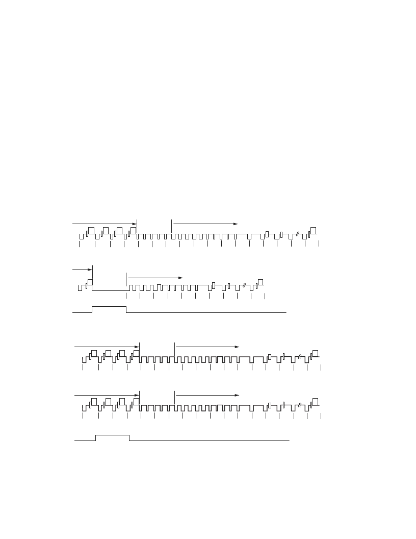
DISPLAY
NO TIMING RESET APPLIED
TIMING RESET APPLIED
START OF FIELD 4 OR 8
F
SC
PHASE = FIELD 4 OR 8
F
SC
PHASE = FIELD 1
TIMING RESET PULSE
307
310
307
1
2
3
4
5
6
7
21
313
320
DISPLAY
START OF FIELD 1
Figure 29. Timing Reset Timing Diagram
NO F
SC
RESET APPLIED
F
SC
PHASE = FIELD 4 OR 8
307
310
313
320
DISPLAY
START OF FIELD 4 OR 8
F
SC
RESET APPLIED
F
SC
RESET PULSE
F
SC
PHASE = FIELD 1
307
310
313
320
DISPLAY
START OF FIELD 4 OR 8
Figure 30. Subcarrier Reset Timing Diagram
This reset signal will have to be held high for a minimum of
one clock cycle.
Since the field counter is not reset, it is recommended that
the reset signal be applied in Field 7 [PAL] or Field 3 [NTSC].
The reset of the phase will then occur on the next field, i.e.,
Field 1, being lined up correctly with the internal counters.
The field count register at Address 7Bh can be used to iden-
tify the number of the active field.
c. In RTC mode, the ADV7312 can be used to lock to an
external video source. The real-time control mode allows the
ADV7312 to automatically alter the subcarrier frequency to
compensate for line length variations. When the part is con-
nected to a device that outputs a digital data stream in the
RTC format, such as an ADV7183A video decoder (see
Figure 31), the part will automatically change to the com-
pensated subcarrier frequency on a line by line basis. This
digital data stream is 67 bits wide and the subcarrier is con-
tained in Bits 0 to 21. Each bit is two clock cycles long. 00h
should be written into all four subcarrier frequency registers
when this mode is used.
相關(guān)PDF資料 |
PDF描述 |
|---|---|
| ADV7320KSTZ | Multiformat 216 MHz Video Encoder with Six NSV 12-Bit DACs |
| ADV7320 | Multiformat 216 MHz Video Encoder with Six NSV 12-Bit DACs |
| ADV7321 | Multiformat 216 MHz Video Encoder with Six NSV 12-Bit DACs |
| ADV7321KSTZ | Multiformat 216 MHz Video Encoder with Six NSV 12-Bit DACs |
| ADV7324 | Multiformat 216 MHz Video Encoder with Six NSV 14-Bit DACs |
相關(guān)代理商/技術(shù)參數(shù) |
參數(shù)描述 |
|---|---|
| ADV7314 | 制造商:AD 制造商全稱:Analog Devices 功能描述:Multiformat 216 MHz Video Encoder with Six NSV 14-Bit DACs |
| ADV7314KST | 制造商:AD 制造商全稱:Analog Devices 功能描述:Multiformat 216 MHz Video Encoder with Six NSV 14-Bit DACs |
| ADV73186702 | 制造商:LG Corporation 功能描述:FRAME ASSEMBLY,DOOR |
| ADV73186703 | 制造商:LG Corporation 功能描述:FRAME ASSEMBLY,DOOR |
| ADV7320 | 制造商:AD 制造商全稱:Analog Devices 功能描述:Multiformat 216 MHz Video Encoder with Six NSV 12-Bit DACs |
發(fā)布緊急采購(gòu),3分鐘左右您將得到回復(fù)。