- 您現(xiàn)在的位置:買賣IC網(wǎng) > PDF目錄16957 > AC162078 (Microchip Technology)HEADER INTRFC MPLAB ICD2 18F1330 PDF資料下載
參數(shù)資料
| 型號: | AC162078 |
| 廠商: | Microchip Technology |
| 文件頁數(shù): | 305/318頁 |
| 文件大?。?/td> | 0K |
| 描述: | HEADER INTRFC MPLAB ICD2 18F1330 |
| 標(biāo)準(zhǔn)包裝: | 1 |
| 附件類型: | 轉(zhuǎn)換接頭 |
| 適用于相關(guān)產(chǎn)品: | ICD2 |
| 產(chǎn)品目錄頁面: | 658 (CN2011-ZH PDF) |
第1頁第2頁第3頁第4頁第5頁第6頁第7頁第8頁第9頁第10頁第11頁第12頁第13頁第14頁第15頁第16頁第17頁第18頁第19頁第20頁第21頁第22頁第23頁第24頁第25頁第26頁第27頁第28頁第29頁第30頁第31頁第32頁第33頁第34頁第35頁第36頁第37頁第38頁第39頁第40頁第41頁第42頁第43頁第44頁第45頁第46頁第47頁第48頁第49頁第50頁第51頁第52頁第53頁第54頁第55頁第56頁第57頁第58頁第59頁第60頁第61頁第62頁第63頁第64頁第65頁第66頁第67頁第68頁第69頁第70頁第71頁第72頁第73頁第74頁第75頁第76頁第77頁第78頁第79頁第80頁第81頁第82頁第83頁第84頁第85頁第86頁第87頁第88頁第89頁第90頁第91頁第92頁第93頁第94頁第95頁第96頁第97頁第98頁第99頁第100頁第101頁第102頁第103頁第104頁第105頁第106頁第107頁第108頁第109頁第110頁第111頁第112頁第113頁第114頁第115頁第116頁第117頁第118頁第119頁第120頁第121頁第122頁第123頁第124頁第125頁第126頁第127頁第128頁第129頁第130頁第131頁第132頁第133頁第134頁第135頁第136頁第137頁第138頁第139頁第140頁第141頁第142頁第143頁第144頁第145頁第146頁第147頁第148頁第149頁第150頁第151頁第152頁第153頁第154頁第155頁第156頁第157頁第158頁第159頁第160頁第161頁第162頁第163頁第164頁第165頁第166頁第167頁第168頁第169頁第170頁第171頁第172頁第173頁第174頁第175頁第176頁第177頁第178頁第179頁第180頁第181頁第182頁第183頁第184頁第185頁第186頁第187頁第188頁第189頁第190頁第191頁第192頁第193頁第194頁第195頁第196頁第197頁第198頁第199頁第200頁第201頁第202頁第203頁第204頁第205頁第206頁第207頁第208頁第209頁第210頁第211頁第212頁第213頁第214頁第215頁第216頁第217頁第218頁第219頁第220頁第221頁第222頁第223頁第224頁第225頁第226頁第227頁第228頁第229頁第230頁第231頁第232頁第233頁第234頁第235頁第236頁第237頁第238頁第239頁第240頁第241頁第242頁第243頁第244頁第245頁第246頁第247頁第248頁第249頁第250頁第251頁第252頁第253頁第254頁第255頁第256頁第257頁第258頁第259頁第260頁第261頁第262頁第263頁第264頁第265頁第266頁第267頁第268頁第269頁第270頁第271頁第272頁第273頁第274頁第275頁第276頁第277頁第278頁第279頁第280頁第281頁第282頁第283頁第284頁第285頁第286頁第287頁第288頁第289頁第290頁第291頁第292頁第293頁第294頁第295頁第296頁第297頁第298頁第299頁第300頁第301頁第302頁第303頁第304頁當(dāng)前第305頁第306頁第307頁第308頁第309頁第310頁第311頁第312頁第313頁第314頁第315頁第316頁第317頁第318頁
PIC18F1230/1330
2009 Microchip Technology Inc.
DS39758D-page 87
10.0
I/O PORTS
Depending on the device selected and features
enabled, there are up to five ports available. Some pins
of the I/O ports are multiplexed with an alternate
function from the peripheral features on the device. In
general, when a peripheral is enabled, that pin may not
be used as a general purpose I/O pin.
Each port has three registers for its operation. These
registers are:
TRIS register (Data Direction register)
PORT register (reads the levels on the pins of the
device)
LAT register (Output Latch register)
The Output Latch (LAT register) is useful for read-
modify-write operations on the value that the I/O pins
are driving.
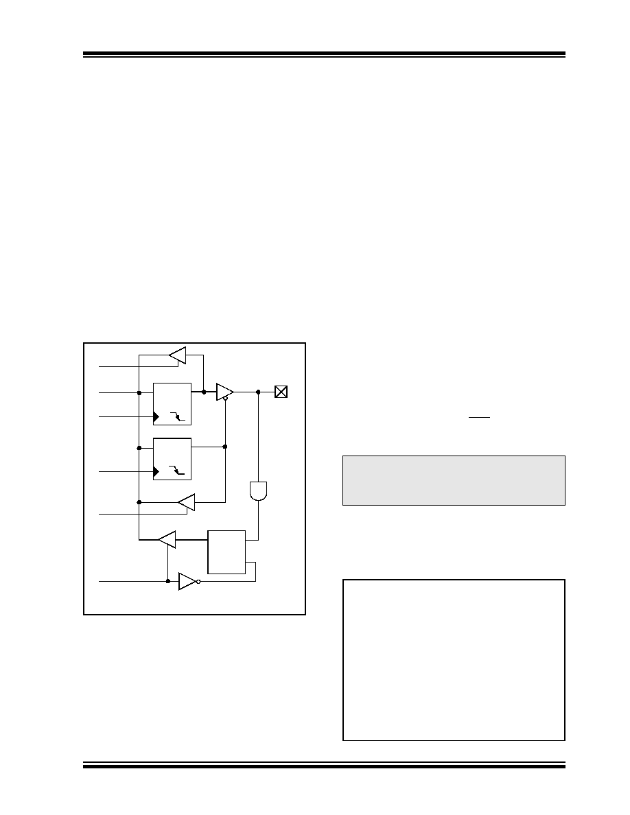
A simplified model of a generic I/O port, without the
interfaces to other peripherals, is shown in Figure 10-1.
FIGURE 10-1:
GENERIC I/O PORT
OPERATION
10.1
PORTA, TRISA and LATA Registers
PORTA is an 8-bit wide, bidirectional port. The
corresponding Data Direction register is TRISA. Setting
a TRISA bit (= 1) will make the corresponding PORTA
pin an input (i.e., put the corresponding output driver in
a high-impedance mode). Clearing a TRISA bit (= 0)
will make the corresponding PORTA pin an output (i.e.,
put the contents of the output latch on the selected pin).
Reading the PORTA register reads the status of the
pins, whereas writing to it, will write to the port latch.
The Output Latch (LATA) register is also memory
mapped. Read-modify-write operations on the LATA
register read and write the latched output value for
PORTA.
Pins RA6 and RA7 are multiplexed with the main
oscillator pins; they are enabled as oscillator or I/O pins
by the selection of the main oscillator in the Configura-
tion register (see Section 20.1 “Configuration Bits”
for details). When they are not used as port pins, RA6
and RA7 and their associated TRIS and LAT bits are
read as ‘0’.
The RA0 pin is multiplexed with one of the analog
inputs, one of the external interrupt inputs, one of the
interrupt-on-change inputs and one of the analog
comparator inputs to become RA0/AN0/INT0/KBI0/
CMP0 pin.
The RA1 pin is multiplexed with one of the analog
inputs, one of the external interrupt inputs and one of
the interrupt-on-change inputs to become RA1/AN1/
INT1/KBI1 pin.
Pins RA2 and RA3 are multiplexed with the Enhanced
USART transmission and reception input (see
for details).
The RA4 pin is multiplexed with the Timer0 module
clock input, one of the analog inputs and the analog
VREF+ input to become the RA4/T0CKI/AN2/VREF+ pin.
The Fault detect input for PWM FLTA is multiplexed with
pins RA5 and RA7. Its placement is decided by clearing
or setting the FLTAMX bit of Configuration Register 3H.
The TRISA register controls the direction of the PORTA
pins, even when they are being used as analog inputs.
The user must ensure the bits in the TRISA register are
maintained set when using them as analog inputs.
EXAMPLE 10-1:
INITIALIZING PORTA
Data
Bus
WR LAT
WR TRIS
RD Port
Data Latch
TRIS Latch
RD TRIS
Input
Buffer
I/O pin(1)
Q
D
CK
Q
D
CK
EN
QD
EN
RD LAT
or Port
Note 1:
I/O pins have diode protection to VDD and VSS.
Note:
On a Power-on Reset, RA0, RA1, RA4
and RA5 are configured as analog inputs
and read as ‘0’. RA2 and RA3 are
configured as digital inputs.
CLRF
PORTA
; Initialize PORTA by
; clearing output
; data latches
CLRF
LATA
; Alternate method
; to clear output
; data latches
MOVLW
07h
; Configure A/D
MOVWF
ADCON1
; for digital inputs
MOVWF
07h
; Configure comparators
MOVWF
CMCON
; for digital input
MOVLW
0CFh
; Value used to
; initialize data
; direction
MOVWF
TRISA
; Set RA<7:6,3:0> as inputs
; RA<5:4> as outputs
相關(guān)PDF資料 |
PDF描述 |
|---|---|
| MLF1005LR33K | INDUCTOR MULTILAYER .33UH 0402 |
| RBM18DRTF | CONN EDGECARD 36POS DIP .156 SLD |
| CBC2518T220M | INDUCTOR 22UH 20% 1007 SMD |
| RCM25DRPS | CONN EDGECARD 50POS DIP .156 SLD |
| LGU2W331MELB | CAP ALUM 330UF 450V 20% SNAP |
相關(guān)代理商/技術(shù)參數(shù) |
參數(shù)描述 |
|---|---|
| AC162079 | 功能描述:插座和適配器 MPLAB ICD 2 64/80L HEADER PIC18F85J90 RoHS:否 制造商:Silicon Labs 產(chǎn)品:Adapter 用于:EM35x |
| AC162083 | 功能描述:插座和適配器 MPLAB ICD 2 8L/14L HEADER PIC16F616 RoHS:否 制造商:Silicon Labs 產(chǎn)品:Adapter 用于:EM35x |
| AC162087 | 功能描述:插座和適配器 MPLAB ICD 2 68/84 HEADER (PIC18F87J50) RoHS:否 制造商:Silicon Labs 產(chǎn)品:Adapter 用于:EM35x |
| AC162088 | 功能描述:插座和適配器 MPLAB ICD 2 PIC24FJ64GA004 28P RoHS:否 制造商:Silicon Labs 產(chǎn)品:Adapter 用于:EM35x |
| AC162088 | 制造商:Microchip Technology Inc 功能描述:MPLAB ICD 2 PIC24FJ64GA004 28P Header |
發(fā)布緊急采購,3分鐘左右您將得到回復(fù)。