- 您現(xiàn)在的位置:買賣IC網(wǎng) > PDF目錄16957 > AC162078 (Microchip Technology)HEADER INTRFC MPLAB ICD2 18F1330 PDF資料下載
參數(shù)資料
| 型號(hào): | AC162078 |
| 廠商: | Microchip Technology |
| 文件頁(yè)數(shù): | 278/318頁(yè) |
| 文件大?。?/td> | 0K |
| 描述: | HEADER INTRFC MPLAB ICD2 18F1330 |
| 標(biāo)準(zhǔn)包裝: | 1 |
| 附件類型: | 轉(zhuǎn)換接頭 |
| 適用于相關(guān)產(chǎn)品: | ICD2 |
| 產(chǎn)品目錄頁(yè)面: | 658 (CN2011-ZH PDF) |
第1頁(yè)第2頁(yè)第3頁(yè)第4頁(yè)第5頁(yè)第6頁(yè)第7頁(yè)第8頁(yè)第9頁(yè)第10頁(yè)第11頁(yè)第12頁(yè)第13頁(yè)第14頁(yè)第15頁(yè)第16頁(yè)第17頁(yè)第18頁(yè)第19頁(yè)第20頁(yè)第21頁(yè)第22頁(yè)第23頁(yè)第24頁(yè)第25頁(yè)第26頁(yè)第27頁(yè)第28頁(yè)第29頁(yè)第30頁(yè)第31頁(yè)第32頁(yè)第33頁(yè)第34頁(yè)第35頁(yè)第36頁(yè)第37頁(yè)第38頁(yè)第39頁(yè)第40頁(yè)第41頁(yè)第42頁(yè)第43頁(yè)第44頁(yè)第45頁(yè)第46頁(yè)第47頁(yè)第48頁(yè)第49頁(yè)第50頁(yè)第51頁(yè)第52頁(yè)第53頁(yè)第54頁(yè)第55頁(yè)第56頁(yè)第57頁(yè)第58頁(yè)第59頁(yè)第60頁(yè)第61頁(yè)第62頁(yè)第63頁(yè)第64頁(yè)第65頁(yè)第66頁(yè)第67頁(yè)第68頁(yè)第69頁(yè)第70頁(yè)第71頁(yè)第72頁(yè)第73頁(yè)第74頁(yè)第75頁(yè)第76頁(yè)第77頁(yè)第78頁(yè)第79頁(yè)第80頁(yè)第81頁(yè)第82頁(yè)第83頁(yè)第84頁(yè)第85頁(yè)第86頁(yè)第87頁(yè)第88頁(yè)第89頁(yè)第90頁(yè)第91頁(yè)第92頁(yè)第93頁(yè)第94頁(yè)第95頁(yè)第96頁(yè)第97頁(yè)第98頁(yè)第99頁(yè)第100頁(yè)第101頁(yè)第102頁(yè)第103頁(yè)第104頁(yè)第105頁(yè)第106頁(yè)第107頁(yè)第108頁(yè)第109頁(yè)第110頁(yè)第111頁(yè)第112頁(yè)第113頁(yè)第114頁(yè)第115頁(yè)第116頁(yè)第117頁(yè)第118頁(yè)第119頁(yè)第120頁(yè)第121頁(yè)第122頁(yè)第123頁(yè)第124頁(yè)第125頁(yè)第126頁(yè)第127頁(yè)第128頁(yè)第129頁(yè)第130頁(yè)第131頁(yè)第132頁(yè)第133頁(yè)第134頁(yè)第135頁(yè)第136頁(yè)第137頁(yè)第138頁(yè)第139頁(yè)第140頁(yè)第141頁(yè)第142頁(yè)第143頁(yè)第144頁(yè)第145頁(yè)第146頁(yè)第147頁(yè)第148頁(yè)第149頁(yè)第150頁(yè)第151頁(yè)第152頁(yè)第153頁(yè)第154頁(yè)第155頁(yè)第156頁(yè)第157頁(yè)第158頁(yè)第159頁(yè)第160頁(yè)第161頁(yè)第162頁(yè)第163頁(yè)第164頁(yè)第165頁(yè)第166頁(yè)第167頁(yè)第168頁(yè)第169頁(yè)第170頁(yè)第171頁(yè)第172頁(yè)第173頁(yè)第174頁(yè)第175頁(yè)第176頁(yè)第177頁(yè)第178頁(yè)第179頁(yè)第180頁(yè)第181頁(yè)第182頁(yè)第183頁(yè)第184頁(yè)第185頁(yè)第186頁(yè)第187頁(yè)第188頁(yè)第189頁(yè)第190頁(yè)第191頁(yè)第192頁(yè)第193頁(yè)第194頁(yè)第195頁(yè)第196頁(yè)第197頁(yè)第198頁(yè)第199頁(yè)第200頁(yè)第201頁(yè)第202頁(yè)第203頁(yè)第204頁(yè)第205頁(yè)第206頁(yè)第207頁(yè)第208頁(yè)第209頁(yè)第210頁(yè)第211頁(yè)第212頁(yè)第213頁(yè)第214頁(yè)第215頁(yè)第216頁(yè)第217頁(yè)第218頁(yè)第219頁(yè)第220頁(yè)第221頁(yè)第222頁(yè)第223頁(yè)第224頁(yè)第225頁(yè)第226頁(yè)第227頁(yè)第228頁(yè)第229頁(yè)第230頁(yè)第231頁(yè)第232頁(yè)第233頁(yè)第234頁(yè)第235頁(yè)第236頁(yè)第237頁(yè)第238頁(yè)第239頁(yè)第240頁(yè)第241頁(yè)第242頁(yè)第243頁(yè)第244頁(yè)第245頁(yè)第246頁(yè)第247頁(yè)第248頁(yè)第249頁(yè)第250頁(yè)第251頁(yè)第252頁(yè)第253頁(yè)第254頁(yè)第255頁(yè)第256頁(yè)第257頁(yè)第258頁(yè)第259頁(yè)第260頁(yè)第261頁(yè)第262頁(yè)第263頁(yè)第264頁(yè)第265頁(yè)第266頁(yè)第267頁(yè)第268頁(yè)第269頁(yè)第270頁(yè)第271頁(yè)第272頁(yè)第273頁(yè)第274頁(yè)第275頁(yè)第276頁(yè)第277頁(yè)當(dāng)前第278頁(yè)第279頁(yè)第280頁(yè)第281頁(yè)第282頁(yè)第283頁(yè)第284頁(yè)第285頁(yè)第286頁(yè)第287頁(yè)第288頁(yè)第289頁(yè)第290頁(yè)第291頁(yè)第292頁(yè)第293頁(yè)第294頁(yè)第295頁(yè)第296頁(yè)第297頁(yè)第298頁(yè)第299頁(yè)第300頁(yè)第301頁(yè)第302頁(yè)第303頁(yè)第304頁(yè)第305頁(yè)第306頁(yè)第307頁(yè)第308頁(yè)第309頁(yè)第310頁(yè)第311頁(yè)第312頁(yè)第313頁(yè)第314頁(yè)第315頁(yè)第316頁(yè)第317頁(yè)第318頁(yè)
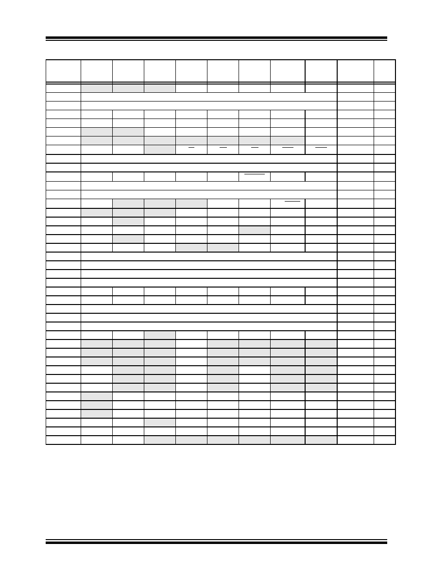
PIC18F1230/1330
DS39758D-page 62
2009 Microchip Technology Inc.
STATUS
—
—N
OV
Z
DC
C
---x xxxx
TMR0H
Timer0 Register High Byte
0000 0000
TMR0L
Timer0 Register Low Byte
xxxx xxxx
T0CON
TMR0ON
T016BIT
T0CS
T0SE
PSA
T0PS2
T0PS1
T0PS0
1111 1111
OSCCON
IDLEN
IRCF2
IRCF1
IRCF0
OSTS
IOFS
SCS1
SCS0
0100 q000
LVDCON
—
IRVST
LVDEN
LVDL3
LVDL2
LVDL1
LVDL0
--00 0101
WDTCON
—
—SWDTEN(7)
---- ---0
RCON
IPEN
SBOREN(1)
—RI
TO
PD
POR
BOR
0q-1 11q0
TMR1H
Timer1 Register High Byte
xxxx xxxx
TMR1L
Timer1 Register Low Byte
xxxx xxxx
T1CON
RD16
T1RUN
T1CKPS1
T1CKPS0
T1OSCEN
T1SYNC
TMR1CS
TMR1ON
0000 0000
ADRESH
A/D Result Register High Byte
xxxx xxxx
ADRESL
A/D Result Register Low Byte
xxxx xxxx
ADCON0
SEVTEN
—
CHS1
CHS0
GO/DONE
ADON
0--- 0000
ADCON1
—
VCFG0
PCFG3
PCFG2
PCFG1
PCFG0
---0 1111
ADCON2
ADFM
—
ACQT2
ACQT1
ACQT0
ADCS2
ADCS1
ADCS0
0-00 0000
BAUDCON
ABDOVF
RCIDL
RXDTP
TXCKP
BRG16
—
WUE
ABDEN
01-0 00-00
CVRCON
CVREN
—
CVRR
CVRSS
CVR3
CVR2
CVR1
CVR0
0-00 0000
CMCON
C2OUT
C1OUT
C0OUT
—
CMEN2
CMEN1
CMEN0
000- -000
SPBRGH
EUSART Baud Rate Generator Register High Byte
0000 0000
SPBRG
EUSART Baud Rate Generator Register Low Byte
0000 0000
RCREG
EUSART Receive Register
0000 0000
TXREG
EUSART Transmit Register
0000 0000
TXSTA
CSRC
TX9
TXEN
SYNC
SENDB
BRGH
TRMT
TX9D
0000 0010
RCSTA
SPEN
RX9
SREN
CREN
ADDEN
FERR
OERR
RX9D
0000 000x
EEADR
EEPROM Address Register
0000 0000
EEDATA
EEPROM Data Register
0000 0000
EECON2
EEPROM Control Register 2 (not a physical register)
0000 0000
EECON1
EEPGD
CFGS
—
FREE
WRERR
WREN
WR
RD
xx-0 x000
IPR3
—
—PTIP
—
---1 ----
PIR3
—
—PTIF
—
---0 ----
PIE3
—
—PTIE
—
---0 ----
IPR2
OSCFIP
—
EEIP
—LVDIP
—
1--1 -1--
PIR2
OSCFIF
—
—EEIF
—LVDIF
—
0--0 -0--
PIE2
OSCFIE
—
EEIE
—LVDIE
—
0--0 -0--
IPR1
—
ADIP
RCIP
TXIP
CMP2IP
CMP1IP
CMP0IP
TMR1IP
-111 1111
PIR1
—
ADIF
RCIF
TXIF
CMP2IF
CMP1IF
CMP0IF
TMR1IF
-000 0000
PIE1
—
ADIE
RCIE
TXIE
CMP2IE
CMP1IE
CMP0IE
TMR1IE
-000 0000
OSCTUNE
INTSRC
PLLEN(2)
—
TUN4
TUN3
TUN2
TUN1
TUN0
00-0 0000
PTCON0
PTOPS3
PTOPS2
PTOPS1
PTOPS0
PTCKPS1
PTCKPS0
PTMOD1
PTMOD0
0000 0000
PTCON1
PTEN
PTDIR
—
00-- ----
TABLE 6-2:
REGISTER FILE SUMMARY (PIC18F1230/1330) (CONTINUED)
File Name
Bit 7
Bit 6
Bit 5
Bit 4
Bit 3
Bit 2
Bit 1
Bit 0
Value on
POR, BOR
Details
on
Page:
Legend:
x
= unknown, u = unchanged, - = unimplemented, q = value depends on condition
Note
1:
The SBOREN bit is only available when the BOREN1:BOREN0 Configuration bits = 01; otherwise, it is disabled and reads
as ‘0’. See Section 5.4 “Brown-out Reset (BOR)”.
2:
The PLLEN bit is only available in specific oscillator configurations; otherwise, it is disabled and reads as ‘0’. See
Section 3.6.4 “PLL in INTOSC Modes”
.
3:
The RA5 bit is only available when Master Clear Reset is disabled (MCLRE Configuration bit = 0); otherwise, RA5 reads as
‘0’. This bit is read-only.
4:
RA6/RA7 and their associated latch and direction bits are individually configured as port pins based on various primary
oscillator modes. When disabled, these bits read as ‘0’.
5:
Bit 7 and bit 6 are cleared by user software or by a POR.
6:
Reset condition of PWMEN bits depends on the PWMPIN Configuration bit of CONFIG3L.
7:
This bit has no effect if the Configuration bit, WDTEN, is enabled.
相關(guān)PDF資料 |
PDF描述 |
|---|---|
| MLF1005LR33K | INDUCTOR MULTILAYER .33UH 0402 |
| RBM18DRTF | CONN EDGECARD 36POS DIP .156 SLD |
| CBC2518T220M | INDUCTOR 22UH 20% 1007 SMD |
| RCM25DRPS | CONN EDGECARD 50POS DIP .156 SLD |
| LGU2W331MELB | CAP ALUM 330UF 450V 20% SNAP |
相關(guān)代理商/技術(shù)參數(shù) |
參數(shù)描述 |
|---|---|
| AC162079 | 功能描述:插座和適配器 MPLAB ICD 2 64/80L HEADER PIC18F85J90 RoHS:否 制造商:Silicon Labs 產(chǎn)品:Adapter 用于:EM35x |
| AC162083 | 功能描述:插座和適配器 MPLAB ICD 2 8L/14L HEADER PIC16F616 RoHS:否 制造商:Silicon Labs 產(chǎn)品:Adapter 用于:EM35x |
| AC162087 | 功能描述:插座和適配器 MPLAB ICD 2 68/84 HEADER (PIC18F87J50) RoHS:否 制造商:Silicon Labs 產(chǎn)品:Adapter 用于:EM35x |
| AC162088 | 功能描述:插座和適配器 MPLAB ICD 2 PIC24FJ64GA004 28P RoHS:否 制造商:Silicon Labs 產(chǎn)品:Adapter 用于:EM35x |
| AC162088 | 制造商:Microchip Technology Inc 功能描述:MPLAB ICD 2 PIC24FJ64GA004 28P Header |
發(fā)布緊急采購(gòu),3分鐘左右您將得到回復(fù)。