- 您現(xiàn)在的位置:買賣IC網(wǎng) > PDF目錄16957 > AC162078 (Microchip Technology)HEADER INTRFC MPLAB ICD2 18F1330 PDF資料下載
參數(shù)資料
| 型號(hào): | AC162078 |
| 廠商: | Microchip Technology |
| 文件頁數(shù): | 125/318頁 |
| 文件大小: | 0K |
| 描述: | HEADER INTRFC MPLAB ICD2 18F1330 |
| 標(biāo)準(zhǔn)包裝: | 1 |
| 附件類型: | 轉(zhuǎn)換接頭 |
| 適用于相關(guān)產(chǎn)品: | ICD2 |
| 產(chǎn)品目錄頁面: | 658 (CN2011-ZH PDF) |
第1頁第2頁第3頁第4頁第5頁第6頁第7頁第8頁第9頁第10頁第11頁第12頁第13頁第14頁第15頁第16頁第17頁第18頁第19頁第20頁第21頁第22頁第23頁第24頁第25頁第26頁第27頁第28頁第29頁第30頁第31頁第32頁第33頁第34頁第35頁第36頁第37頁第38頁第39頁第40頁第41頁第42頁第43頁第44頁第45頁第46頁第47頁第48頁第49頁第50頁第51頁第52頁第53頁第54頁第55頁第56頁第57頁第58頁第59頁第60頁第61頁第62頁第63頁第64頁第65頁第66頁第67頁第68頁第69頁第70頁第71頁第72頁第73頁第74頁第75頁第76頁第77頁第78頁第79頁第80頁第81頁第82頁第83頁第84頁第85頁第86頁第87頁第88頁第89頁第90頁第91頁第92頁第93頁第94頁第95頁第96頁第97頁第98頁第99頁第100頁第101頁第102頁第103頁第104頁第105頁第106頁第107頁第108頁第109頁第110頁第111頁第112頁第113頁第114頁第115頁第116頁第117頁第118頁第119頁第120頁第121頁第122頁第123頁第124頁當(dāng)前第125頁第126頁第127頁第128頁第129頁第130頁第131頁第132頁第133頁第134頁第135頁第136頁第137頁第138頁第139頁第140頁第141頁第142頁第143頁第144頁第145頁第146頁第147頁第148頁第149頁第150頁第151頁第152頁第153頁第154頁第155頁第156頁第157頁第158頁第159頁第160頁第161頁第162頁第163頁第164頁第165頁第166頁第167頁第168頁第169頁第170頁第171頁第172頁第173頁第174頁第175頁第176頁第177頁第178頁第179頁第180頁第181頁第182頁第183頁第184頁第185頁第186頁第187頁第188頁第189頁第190頁第191頁第192頁第193頁第194頁第195頁第196頁第197頁第198頁第199頁第200頁第201頁第202頁第203頁第204頁第205頁第206頁第207頁第208頁第209頁第210頁第211頁第212頁第213頁第214頁第215頁第216頁第217頁第218頁第219頁第220頁第221頁第222頁第223頁第224頁第225頁第226頁第227頁第228頁第229頁第230頁第231頁第232頁第233頁第234頁第235頁第236頁第237頁第238頁第239頁第240頁第241頁第242頁第243頁第244頁第245頁第246頁第247頁第248頁第249頁第250頁第251頁第252頁第253頁第254頁第255頁第256頁第257頁第258頁第259頁第260頁第261頁第262頁第263頁第264頁第265頁第266頁第267頁第268頁第269頁第270頁第271頁第272頁第273頁第274頁第275頁第276頁第277頁第278頁第279頁第280頁第281頁第282頁第283頁第284頁第285頁第286頁第287頁第288頁第289頁第290頁第291頁第292頁第293頁第294頁第295頁第296頁第297頁第298頁第299頁第300頁第301頁第302頁第303頁第304頁第305頁第306頁第307頁第308頁第309頁第310頁第311頁第312頁第313頁第314頁第315頁第316頁第317頁第318頁
PIC18F1230/1330
DS39758D-page 210
2009 Microchip Technology Inc.
20.5.2
DATA EEPROM
CODE PROTECTION
The entire data EEPROM is protected from external
reads and writes by two bits: CPD and WRTD. CPD
inhibits external reads and writes of data EEPROM.
WRTD inhibits internal and external writes to data
EEPROM. The CPU can always read data EEPROM
under normal operation, regardless of the protection bit
settings.
20.5.3
CONFIGURATION REGISTER
PROTECTION
The Configuration registers can be write-protected.
The WRTC bit controls protection of the Configuration
registers. In normal execution mode, the WRTC bit is
read-only. WRTC can only be written via ICSP
operation or an external programmer.
20.6
ID Locations
Eight memory locations (200000h-200007h) are
designated as ID locations, where the user can store
checksum or other code identification numbers. These
locations are both readable and writable during normal
execution through the TBLRD and TBLWT instructions
or during program/verify. The ID locations can be read
when the device is code-protected.
20.7
In-Circuit Serial Programming
PIC18F1230/1330 microcontrollers can be serially
programmed while in the end application circuit. This is
simply done with two lines for clock and data and three
other lines for power, ground and the programming
voltage. This allows customers to manufacture boards
with unprogrammed devices and then program the
microcontroller just before shipping the product. This
also allows the most recent firmware or a custom
firmware to be programmed.
20.8
In-Circuit Debugger
When the BKBUG Configuration bit is programmed to
a ‘0’, the In-Circuit Debugger functionality is enabled.
This function allows simple debugging functions when
used with MPLAB IDE. When the microcontroller has
this feature enabled, some resources are not available
for general use. Table 20-4 shows which resources are
required by the background debugger.
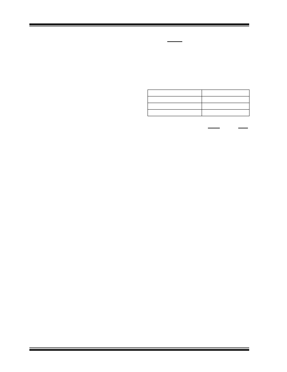
TABLE 20-4:
DEBUGGER RESOURCES
To use the In-Circuit Debugger function of the microcon-
troller, the design must implement In-Circuit Serial
Programming connections to MCLR/VPP/RA5/FLTA,
VDD, VSS, RB7/PWM5/PGD and RB6/PWM4/PGC. This
will interface to the In-Circuit Debugger module available
from Microchip or one of the third party development tool
companies.
20.9
Single-Supply ICSP Programming
The PIC18F1230/1330 device family does not support
Low-Voltage ICSP Programming or LVP. This device
family can only be programmed using high-voltage ICSP
programming.
For
more
details,
refer
to
the
“PIC18F1230/1330 Flash Microcontroller Programming
Specification”
(DS39752).
Memory that is not code-protected can be erased using
either a block erase, or erased row by row, then written
at any specified VDD. If code-protected memory is to be
erased, a block erase is required.
I/O pins:
RB6, RB7
Stack:
2 levels
Program Memory:
512 bytes
Data Memory:
10 bytes
相關(guān)PDF資料 |
PDF描述 |
|---|---|
| MLF1005LR33K | INDUCTOR MULTILAYER .33UH 0402 |
| RBM18DRTF | CONN EDGECARD 36POS DIP .156 SLD |
| CBC2518T220M | INDUCTOR 22UH 20% 1007 SMD |
| RCM25DRPS | CONN EDGECARD 50POS DIP .156 SLD |
| LGU2W331MELB | CAP ALUM 330UF 450V 20% SNAP |
相關(guān)代理商/技術(shù)參數(shù) |
參數(shù)描述 |
|---|---|
| AC162079 | 功能描述:插座和適配器 MPLAB ICD 2 64/80L HEADER PIC18F85J90 RoHS:否 制造商:Silicon Labs 產(chǎn)品:Adapter 用于:EM35x |
| AC162083 | 功能描述:插座和適配器 MPLAB ICD 2 8L/14L HEADER PIC16F616 RoHS:否 制造商:Silicon Labs 產(chǎn)品:Adapter 用于:EM35x |
| AC162087 | 功能描述:插座和適配器 MPLAB ICD 2 68/84 HEADER (PIC18F87J50) RoHS:否 制造商:Silicon Labs 產(chǎn)品:Adapter 用于:EM35x |
| AC162088 | 功能描述:插座和適配器 MPLAB ICD 2 PIC24FJ64GA004 28P RoHS:否 制造商:Silicon Labs 產(chǎn)品:Adapter 用于:EM35x |
| AC162088 | 制造商:Microchip Technology Inc 功能描述:MPLAB ICD 2 PIC24FJ64GA004 28P Header |
發(fā)布緊急采購,3分鐘左右您將得到回復(fù)。