- 您現(xiàn)在的位置:買賣IC網(wǎng) > PDF目錄360524 > 7643 IrDA. protocol handler plus endec for DCE Apps, -40C to +85C, 18-SOIC 300mil, TUBE PDF資料下載
參數(shù)資料
| 型號: | 7643 |
| 英文描述: | IrDA. protocol handler plus endec for DCE Apps, -40C to +85C, 18-SOIC 300mil, TUBE |
| 中文描述: | 7643Group數(shù)據(jù)表數(shù)據(jù)表1369K/JUL.30.03 |
| 文件頁數(shù): | 4/120頁 |
| 文件大小: | 1369K |
| 代理商: | 7643 |
第1頁第2頁第3頁當前第4頁第5頁第6頁第7頁第8頁第9頁第10頁第11頁第12頁第13頁第14頁第15頁第16頁第17頁第18頁第19頁第20頁第21頁第22頁第23頁第24頁第25頁第26頁第27頁第28頁第29頁第30頁第31頁第32頁第33頁第34頁第35頁第36頁第37頁第38頁第39頁第40頁第41頁第42頁第43頁第44頁第45頁第46頁第47頁第48頁第49頁第50頁第51頁第52頁第53頁第54頁第55頁第56頁第57頁第58頁第59頁第60頁第61頁第62頁第63頁第64頁第65頁第66頁第67頁第68頁第69頁第70頁第71頁第72頁第73頁第74頁第75頁第76頁第77頁第78頁第79頁第80頁第81頁第82頁第83頁第84頁第85頁第86頁第87頁第88頁第89頁第90頁第91頁第92頁第93頁第94頁第95頁第96頁第97頁第98頁第99頁第100頁第101頁第102頁第103頁第104頁第105頁第106頁第107頁第108頁第109頁第110頁第111頁第112頁第113頁第114頁第115頁第116頁第117頁第118頁第119頁第120頁
Rev.1.00 Jul 30, 2003 page 4 of 119
7643 Group
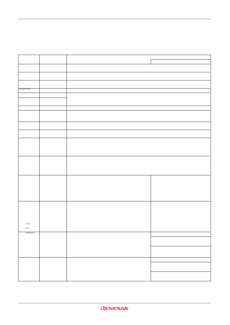
P5
0
/X
CIN
,
P5
1
/T
OUT
/
X
COUT
,
P5
2
,P5
3
,P5
4
,
P5
5
,P5
6
,P5
7
Apply 4.15 V – 5.25 V for 5 V version or 3.00 V – 3.60 V for 3 V version to the Vcc pin. Apply 0 V to the
Vss pin.
This controls the MCU operating mode. Connect this pin to Vss. If connecting this pin to Vcc, the
internal ROM is inhibited. In the flash memory version this pin functions as a V
PP
power supply input pin.
These pins are the power supply inputs for analog circuitry.
Reset input pin for active “L.”
Connect a ceramic resonator or a quartz-crystal oscillator between the X
IN
and X
OUT
pins to set the
oscillation frequency.
If an external clock is used, connect the clock source to the X
IN
pin and leave the X
OUT
pin open.
Loop filter for the frequency synthesizer.
It is a capacitor connection pin for built-in DC-DC converter. At Vcc=5 V, use built-in DC-DC converter
by permitting a USB line driver and connect a capacitor. Refer to "Notes on use" for details. Built-in DC-
DC converter cannot be used at Vcc = 3.3 V. Supply 3.3V power supply to this pin from the externals.
USB D+ voltage signal port. Connect a 27 to 33
(recommended) resistor in series.
USB D- voltage signal port. Connect a 27 to 33
(recommended) resistor in series.
8-bit I/O port.
CMOS compatible input level.
CMOS 3-state output structure.
I/O direction register allows each pin to be individually programmed as either input or output.
When connecting an external memory, these function as the address bus.
8-bit I/O port.
CMOS compatible input level.
CMOS 3-state output structure.
I/O direction register allows each pin to be individually programmed as either input or output.
When connecting an external memory, these function as the address bus.
Key-on wake-up interrupt input pin
V
CC
, V
SS
CNVss/V
PP
AVss/AVcc
RESET
X
IN
X
OUT
LPF
Ext. Cap.
USB D+
USB D-
P0
0
/AB
0
–
P0
7
/AB
7
Name
Power source
CNVss
Analog power
supply
Reset input
Clock input
Clock output
LPF
3.3 V line power
supply
USB D+
USB D-
Function except a port function
PIN DESCRIPTION
Table 1 Pin description (1)
Function
P1
0
/AB
8
–
P1
7
/AB
15
P2
0
/DB
0
–
P2
7
/DB
7
8-bit I/O port.
CMOS compatible input level or VIHL input level.
CMOS 3-state output structure.
I/O direction register allows each pin to be individually
programmed as either input or output.
When connecting an external memory, these function as
the data bus.
8-bit I/O port.
CMOS compatible input level.
CMOS 3-state output structure.
I/O direction register allows each pin to be individually
programmed as either input or output.
When connecting an external memory, these function as
the control bus.
P3
0
/RDY,
P3
1
, P3
2
,
P3
3
/DMA
OUT
,
P3
4
/
φ
OUT
,
P3
5
/SYNC
OUT
,
P3
6
/WR,
P3
7
/RD
P4
0
/EDMA,
P4
1
/INT
0
,
P4
2
/INT
1
,
P4
3
,P4
4
8-bit I/O port.
CMOS compatible input level.
CMOS 3-state output structure.
I/O direction register allows each pin to be individually
programmed as either input or output.
When connecting an external memory, these function as
the control bus.
8-bit I/O port.
CMOS compatible input level.
CMOS 3-state output structure.
I/O direction register allows each pin to be individually
programmed as either input or output.
I/O port P0
I/O port P1
I/O port P2
I/O port P3
(See Remarks.)
External memory control pin
External memory control pin
External interrupt pin
Sub-clock generating input pin
Timers 1, 2 pulse output pins
Sub-clock generating output pin
Pin
I/O port P4
I/O port P5
相關PDF資料 |
PDF描述 |
|---|---|
| 765-11-(SERIES) | Analog IC |
| 765-11-20K | Analog IC |
| 765-11-25A | Analog IC |
| 765-11E | 8 BIT INPUT/OUTPUT EXPANDER, I2C INTERFACE, -40C to +125C, 20-QFN, TUBE |
| 765-11R | 8-bit I/O Expander with I2C Interface., -40C to +125C, 18-SOIC 300mil, TUBE |
相關代理商/技術參數(shù) |
參數(shù)描述 |
|---|---|
| 764-3"x36yd-Red | 功能描述:膠帶 764 RED 3X36 YD BULK RoHS:否 制造商:3M Electronic Specialty 產(chǎn)品:Tapes 類型:Shielding 描述/功能:EMI/RFI Foil Shielding Tape 顏色: 材料:Copper Foil 寬度:1 in x 18 yds |
| 764-3"x36yd-White | 功能描述:膠帶 WHITE 3X36YD BULK RoHS:否 制造商:3M Electronic Specialty 產(chǎn)品:Tapes 類型:Shielding 描述/功能:EMI/RFI Foil Shielding Tape 顏色: 材料:Copper Foil 寬度:1 in x 18 yds |
| 764-3"x36yd-Yellow | 功能描述:膠帶 764 YELLOW 3X36 YD BULK RoHS:否 制造商:3M Electronic Specialty 產(chǎn)品:Tapes 類型:Shielding 描述/功能:EMI/RFI Foil Shielding Tape 顏色: 材料:Copper Foil 寬度:1 in x 18 yds |
| 7643_06 | 制造商:RENESAS 制造商全稱:Renesas Technology Corp 功能描述:8-BIT SINGLE-CHIP MICROCOMPUTER |
| 76430 | 制造商:Brady Corporation 功能描述:TAPE, BARRICADE, BLACK/PHOSPHORESCENT, 2INX5YD; Tape Type:Safety, Hazard Warning; Tape Backing Material:Polyester Film; Tape Width - Metric:50.8mm; Tape Width - Imperial:2"; Tape Length - Metric:4.572m; Tape Length - Imperial:5yard ;RoHS Compliant: NA |
發(fā)布緊急采購,3分鐘左右您將得到回復。