- 您現(xiàn)在的位置:買賣IC網(wǎng) > PDF目錄1973 > XA3SD3400A-4FGG676I (Xilinx Inc)SPARTAN-3ADSP FPGA 3400K 676FBGA PDF資料下載
參數(shù)資料
| 型號: | XA3SD3400A-4FGG676I |
| 廠商: | Xilinx Inc |
| 文件頁數(shù): | 37/58頁 |
| 文件大小: | 0K |
| 描述: | SPARTAN-3ADSP FPGA 3400K 676FBGA |
| 產(chǎn)品培訓(xùn)模塊: | Extended Spartan 3A FPGA Family |
| 標(biāo)準(zhǔn)包裝: | 40 |
| 系列: | Spartan®-3A DSP XA |
| LAB/CLB數(shù): | 5968 |
| 邏輯元件/單元數(shù): | 53712 |
| RAM 位總計: | 2322432 |
| 輸入/輸出數(shù): | 469 |
| 門數(shù): | 3400000 |
| 電源電壓: | 1.14 V ~ 1.26 V |
| 安裝類型: | 表面貼裝 |
| 工作溫度: | -40°C ~ 100°C |
| 封裝/外殼: | 676-BGA |
| 供應(yīng)商設(shè)備封裝: | 676-FBGA(27x27) |
第1頁第2頁第3頁第4頁第5頁第6頁第7頁第8頁第9頁第10頁第11頁第12頁第13頁第14頁第15頁第16頁第17頁第18頁第19頁第20頁第21頁第22頁第23頁第24頁第25頁第26頁第27頁第28頁第29頁第30頁第31頁第32頁第33頁第34頁第35頁第36頁當(dāng)前第37頁第38頁第39頁第40頁第41頁第42頁第43頁第44頁第45頁第46頁第47頁第48頁第49頁第50頁第51頁第52頁第53頁第54頁第55頁第56頁第57頁第58頁
XA Spartan-3A DSP Automotive FPGA Family Data Sheet
DS705 (v2.0) April 18, 2011
Product Specification
42
Digital Clock Manager Timing
For specification purposes, the DCM consists of three key components: the Delay-Locked Loop (DLL), the Digital Frequency
Synthesizer (DFS), and the Phase Shifter (PS).
Aspects of DLL operation play a role in all DCM applications. All such applications inevitably use the CLKIN and the CLKFB
inputs connected to either the CLK0 or the CLK2X feedback, respectively. Thus, specifications in the DLL tables (Table 37
and Table 38) apply to any application that only employs the DLL component. When the DFS and/or the PS components are
used together with the DLL, then the specifications listed in the DFS and PS tables (Table 39 through Table 42) supersede
any corresponding ones in the DLL tables. DLL specifications that do not change with the addition of DFS or PS functions
Period jitter and cycle-cycle jitter are two of many different ways of specifying clock jitter. Both specifications describe
statistical variation from a mean value.
Period jitter is the worst-case deviation from the ideal clock period over a collection of millions of samples. In a histogram of
period jitter, the mean value is the clock period.
Cycle-cycle jitter is the worst-case difference in clock period between adjacent clock cycles in the collection of clock periods
sampled. In a histogram of cycle-cycle jitter, the mean value is zero.
Delay-Locked Loop
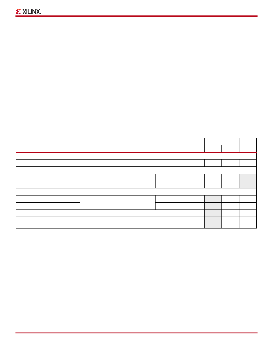
Table 37: Recommended Operating Conditions for the DLL
Symbol
Description
Speed Grade: -4
Units
Min
Max
Input Frequency Ranges
FCLKIN
CLKIN_FREQ_DLL
Frequency of the CLKIN clock input
5(2)
250(3)
MHz
Input Pulse Requirements
CLKIN_PULSE
CLKIN pulse width as a percentage of the
CLKIN period
FCLKIN 150 MHz
40%
60%
–
FCLKIN 150 MHz
45%
55%
–
Input Clock Jitter Tolerance and Delay Path Variation(4)
CLKIN_CYC_JITT_DLL_LF
Cycle-to-cycle jitter at the CLKIN input
FCLKIN 150 MHz
–±300
ps
CLKIN_CYC_JITT_DLL_HF
FCLKIN 150 MHz
–±150
ps
CLKIN_PER_JITT_DLL
Period jitter at the CLKIN input
–±1
ns
CLKFB_DELAY_VAR_EXT
Allowable variation of off-chip feedback delay from the DCM output to
the CLKFB input
–±1
ns
Notes:
1.
DLL specifications apply when any of the DLL outputs (CLK0, CLK90, CLK180, CLK270, CLK2X, CLK2X180, or CLKDV) are in use.
2.
The DFS, when operating independently of the DLL, supports lower FCLKIN frequencies. See Table 39.
3.
To support double the maximum effective FCLKIN limit, set the CLKIN_DIVIDE_BY_2 attribute to TRUE. This attribute divides the incoming
clock period by two as it enters the DCM. The CLK2X output reproduces the clock frequency provided on the CLKIN input.
4.
CLKIN input jitter beyond these limits might cause the DCM to lose lock.
5.
The DCM specifications are guaranteed when both adjacent DCMs are locked.
相關(guān)PDF資料 |
PDF描述 |
|---|---|
| XA6SLX75T-3FGG484Q | IC FPGA SPARTAN 6 484FGGBGA |
| XA95144XL-15CSG144I | IC CPLD 144MC 117 I/O 144CSBGA |
| XAM1808AZCE4 | IC ARM PROCESSOR 361NFBGA |
| XC1765ESOG8C | IC PROM SERIAL 65K 8-SOIC |
| XC17S200AVQ44I | IC PROM SER 200000 I-TEMP 44VQFP |
相關(guān)代理商/技術(shù)參數(shù) |
參數(shù)描述 |
|---|---|
| X-A4A-300L | 制造商:Leach International Corporation 功能描述:MID RANGE - Bulk |
| X-A4C-300M | 制造商:Leach International Corporation 功能描述:MID RANGE - Bulk |
| X-A4M-300L | 制造商:Leach International Corporation 功能描述:MID RANGE - Bulk |
| X-A4M-300M | 制造商:Leach International Corporation 功能描述:MID RANGE - Bulk |
| X-A4N | 制造商:Leach International Corporation 功能描述:MID RANGE - Bulk |
發(fā)布緊急采購,3分鐘左右您將得到回復(fù)。