- 您現(xiàn)在的位置:買賣IC網(wǎng) > PDF目錄1973 > XA3SD3400A-4FGG676I (Xilinx Inc)SPARTAN-3ADSP FPGA 3400K 676FBGA PDF資料下載
參數(shù)資料
| 型號: | XA3SD3400A-4FGG676I |
| 廠商: | Xilinx Inc |
| 文件頁數(shù): | 24/58頁 |
| 文件大?。?/td> | 0K |
| 描述: | SPARTAN-3ADSP FPGA 3400K 676FBGA |
| 產品培訓模塊: | Extended Spartan 3A FPGA Family |
| 標準包裝: | 40 |
| 系列: | Spartan®-3A DSP XA |
| LAB/CLB數(shù): | 5968 |
| 邏輯元件/單元數(shù): | 53712 |
| RAM 位總計: | 2322432 |
| 輸入/輸出數(shù): | 469 |
| 門數(shù): | 3400000 |
| 電源電壓: | 1.14 V ~ 1.26 V |
| 安裝類型: | 表面貼裝 |
| 工作溫度: | -40°C ~ 100°C |
| 封裝/外殼: | 676-BGA |
| 供應商設備封裝: | 676-FBGA(27x27) |
第1頁第2頁第3頁第4頁第5頁第6頁第7頁第8頁第9頁第10頁第11頁第12頁第13頁第14頁第15頁第16頁第17頁第18頁第19頁第20頁第21頁第22頁第23頁當前第24頁第25頁第26頁第27頁第28頁第29頁第30頁第31頁第32頁第33頁第34頁第35頁第36頁第37頁第38頁第39頁第40頁第41頁第42頁第43頁第44頁第45頁第46頁第47頁第48頁第49頁第50頁第51頁第52頁第53頁第54頁第55頁第56頁第57頁第58頁
XA Spartan-3A DSP Automotive FPGA Family Data Sheet
DS705 (v2.0) April 18, 2011
Product Specification
30
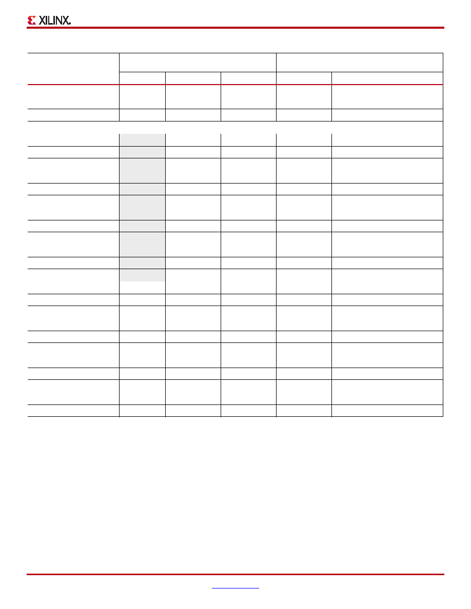
The capacitive load (CL) is connected between the output and GND. The Output timing for all standards, as published in the
speed files and the data sheet, is always based on a CL value of zero. High-impedance probes (less than 1 pF) are used for
all measurements. Any delay that the test fixture might contribute to test measurements is subtracted from those
measurements to produce the final timing numbers as published in the speed files and data sheet.
SSTL2_II
1.25
VREF – 0.75
VREF + 0.75
25
1.25
VREF
SSTL3_I
1.5
VREF – 0.75
VREF + 0.75
50
1.5
VREF
SSTL3_II
1.5
VREF – 0.75
VREF + 0.75
25
1.5
VREF
Differential
LVDS_25
–VICM – 0.125
VICM + 0.125
50
1.2
VICM
LVDS_33
–VICM – 0.125
VICM + 0.125
50
1.2
VICM
BLVDS_25
–VICM – 0.125
VICM + 0.125
1M
0
VICM
MINI_LVDS_25
–VICM – 0.125
VICM + 0.125
50
1.2
VICM
MINI_LVDS_33
–VICM – 0.125
VICM + 0.125
50
1.2
VICM
LVPECL_25
–VICM – 0.3
VICM + 0.3
N/A
VICM
LVPECL_33
–VICM – 0.3
VICM + 0.3
N/A
VICM
RSDS_25
–VICM – 0.1
VICM + 0.1
50
1.2
VICM
RSDS_33
–VICM – 0.1
VICM + 0.1
50
1.2
VICM
TMDS_33
–VICM – 0.1
VICM + 0.1
50
3.3
VICM
PPDS_25
–VICM – 0.1
VICM + 0.1
50
0.8
VICM
PPDS_33
–VICM – 0.1
VICM + 0.1
50
0.8
VICM
DIFF_HSTL_I
0.9
VREF – 0.5
VREF + 0.5
50
0.9
VREF
DIFF_HSTL_III
0.9
VREF – 0.5
VREF + 0.5
50
0.9
VREF
DIFF_HSTL_I_18
0.9
VREF – 0.5
VREF + 0.5
50
0.9
VREF
DIFF_HSTL_II_18
0.9
VREF – 0.5
VREF + 0.5
50
0.9
VREF
DIFF_HSTL_III_18
1.1
VREF – 0.5
VREF + 0.5
50
1.8
VREF
DIFF_SSTL18_I
0.9
VREF – 0.5
VREF + 0.5
50
0.9
VREF
DIFF_SSTL18_II
0.9
VREF – 0.5
VREF + 0.5
50
0.9
VREF
DIFF_SSTL2_I
1.25
VREF – 0.5
VREF + 0.5
50
1.25
VREF
DIFF_SSTL2_II
1.25
VREF – 0.5
VREF + 0.5
50
1.25
VREF
DIFF_SSTL3_I
1.5
VREF – 0.5
VREF + 0.5
50
1.5
VREF
DIFF_SSTL3_II
1.5
VREF – 0.5
VREF + 0.5
50
1.5
VREF
Notes:
1.
Descriptions of the relevant symbols are as follows:
VREF – The reference voltage for setting the input switching threshold
VICM – The common mode input voltage
VM – Voltage of measurement point on signal transition
VL – Low-level test voltage at Input pin
VH – High-level test voltage at Input pin
RT – Effective termination resistance, which takes on a value of 1 M when no parallel termination is required
VT – Termination voltage
2.
The load capacitance (CL) at the Output pin is 0 pF for all signal standards.
3.
According to the PCI specification.
Table 27: Test Methods for Timing Measurement at I/Os (Cont’d)
Signal Standard
(IOSTANDARD)
Inputs
Outputs
Inputs and
Outputs
VREF (V)
VL (V)
VH (V)
RT ()VT (V)
VM (V)
相關PDF資料 |
PDF描述 |
|---|---|
| XA6SLX75T-3FGG484Q | IC FPGA SPARTAN 6 484FGGBGA |
| XA95144XL-15CSG144I | IC CPLD 144MC 117 I/O 144CSBGA |
| XAM1808AZCE4 | IC ARM PROCESSOR 361NFBGA |
| XC1765ESOG8C | IC PROM SERIAL 65K 8-SOIC |
| XC17S200AVQ44I | IC PROM SER 200000 I-TEMP 44VQFP |
相關代理商/技術參數(shù) |
參數(shù)描述 |
|---|---|
| X-A4A-300L | 制造商:Leach International Corporation 功能描述:MID RANGE - Bulk |
| X-A4C-300M | 制造商:Leach International Corporation 功能描述:MID RANGE - Bulk |
| X-A4M-300L | 制造商:Leach International Corporation 功能描述:MID RANGE - Bulk |
| X-A4M-300M | 制造商:Leach International Corporation 功能描述:MID RANGE - Bulk |
| X-A4N | 制造商:Leach International Corporation 功能描述:MID RANGE - Bulk |
發(fā)布緊急采購,3分鐘左右您將得到回復。