- 您現(xiàn)在的位置:買賣IC網(wǎng) > PDF目錄98286 > TPU3035PK TELETEXT DECODER, PDIP40 PDF資料下載
參數(shù)資料
| 型號: | TPU3035PK |
| 元件分類: | 圖文 |
| 英文描述: | TELETEXT DECODER, PDIP40 |
| 封裝: | PLASTIC, DIP-40 |
| 文件頁數(shù): | 9/72頁 |
| 文件大小: | 347K |
| 代理商: | TPU3035PK |
第1頁第2頁第3頁第4頁第5頁第6頁第7頁第8頁當(dāng)前第9頁第10頁第11頁第12頁第13頁第14頁第15頁第16頁第17頁第18頁第19頁第20頁第21頁第22頁第23頁第24頁第25頁第26頁第27頁第28頁第29頁第30頁第31頁第32頁第33頁第34頁第35頁第36頁第37頁第38頁第39頁第40頁第41頁第42頁第43頁第44頁第45頁第46頁第47頁第48頁第49頁第50頁第51頁第52頁第53頁第54頁第55頁第56頁第57頁第58頁第59頁第60頁第61頁第62頁第63頁第64頁第65頁第66頁第67頁第68頁第69頁第70頁第71頁第72頁
TPU 3035, TPU 3040, TPU 3050
PRELIMINARY DATA SHEET
17
Micronas
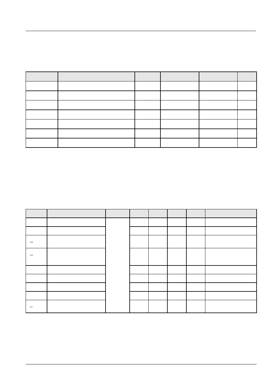
3.6. Electrical Characteristics
All voltages refer to ground.
3.6.1. Absolute Maximum Ratings
Symbol
Parameter
Pin No.
Min.
Max.
Unit
TA
Ambient Operating Temperature
–
0
65
°C
TS
Storage Temperature
–
*40
125
°C
VDSUP
Digital Supply Voltage
34
*0.3
6
V
VASUP
Analog Supply Voltage
41
*0.3
6
V
VDI
Digital Input Voltage
*0.3
VDSUP )0.3
V
VAI
Analog Input Voltage
*0.3
VASUP )0.3
V
IO
Output Current
*10
10
mA
Stresses beyond those listed in the “Absolute Maximum Ratings” may cause permanent damage to the device. This
is a stress rating only. Functional operation of the device at these or any other conditions beyond those indicated in the
“Recommended Operating Conditions/Characteristics” of this specification is not implied. Exposure to absolute maxi-
mum ratings conditions for extended periods may affect device reliability.
3.6.2. Recommended Crystal Characteristics
Symbol
Parameter
Pin No.
Min.
Typ.
Max.
Unit
Test Conditions
TA
Ambient Operating Temperature
27, 28
0
–
65
°C
f0
Parallel Resonance Frequency
–
20.25
–
MHz
CL = 30 pF, TA = 25 °C
f
f0
Frequency Tolerance
–
± 50
ppm
TA = 25 °C
f
Frequency
Deviation
versus
Temperature
–
± 50
ppm
over operating temperature
range with respect to fre-
quency at 25
°C
Rr
Series Resistance
–
30
C0
Static Capacitance
–
8
pF
C1
Dynamic Capacitance
10
–
30
fF
PD
Rated Drive Level
–
0.2
–
mW
f0
fH
Spurious Frequency Attenuation
3
–
dB
相關(guān)PDF資料 |
PDF描述 |
|---|---|
| TPU3035PO | TELETEXT DECODER, PDIP52 |
| TPU3035PQ | TELETEXT DECODER, PQCC44 |
| TPU3050PK | TELETEXT DECODER, PDIP40 |
| TPU3050PO | TELETEXT DECODER, PDIP52 |
| TPU3050PQ | TELETEXT DECODER, PQCC44 |
相關(guān)代理商/技術(shù)參數(shù) |
參數(shù)描述 |
|---|---|
| TPU304 | 制造商:未知廠家 制造商全稱:未知廠家 功能描述:TRANSISTOR | JFET | P-CHANNEL | 30MA I(DSS) | TO-226AA |
| TPU3040 | 制造商:MICRONAS 制造商全稱:MICRONAS 功能描述:Teletext Processors |
| TPU3040(DIP40) | 制造商:未知廠家 制造商全稱:未知廠家 功能描述:Teletext Circuit |
| TPU3040(PDIP40) | 制造商:未知廠家 制造商全稱:未知廠家 功能描述:Microprocessor |
| TPU3040(PSDIP52) | 制造商:未知廠家 制造商全稱:未知廠家 功能描述:Microprocessor |
發(fā)布緊急采購,3分鐘左右您將得到回復(fù)。