- 您現(xiàn)在的位置:買賣IC網(wǎng) > PDF目錄98286 > TPU3035PK TELETEXT DECODER, PDIP40 PDF資料下載
參數(shù)資料
| 型號(hào): | TPU3035PK |
| 元件分類: | 圖文 |
| 英文描述: | TELETEXT DECODER, PDIP40 |
| 封裝: | PLASTIC, DIP-40 |
| 文件頁(yè)數(shù): | 72/72頁(yè) |
| 文件大小: | 347K |
| 代理商: | TPU3035PK |
第1頁(yè)第2頁(yè)第3頁(yè)第4頁(yè)第5頁(yè)第6頁(yè)第7頁(yè)第8頁(yè)第9頁(yè)第10頁(yè)第11頁(yè)第12頁(yè)第13頁(yè)第14頁(yè)第15頁(yè)第16頁(yè)第17頁(yè)第18頁(yè)第19頁(yè)第20頁(yè)第21頁(yè)第22頁(yè)第23頁(yè)第24頁(yè)第25頁(yè)第26頁(yè)第27頁(yè)第28頁(yè)第29頁(yè)第30頁(yè)第31頁(yè)第32頁(yè)第33頁(yè)第34頁(yè)第35頁(yè)第36頁(yè)第37頁(yè)第38頁(yè)第39頁(yè)第40頁(yè)第41頁(yè)第42頁(yè)第43頁(yè)第44頁(yè)第45頁(yè)第46頁(yè)第47頁(yè)第48頁(yè)第49頁(yè)第50頁(yè)第51頁(yè)第52頁(yè)第53頁(yè)第54頁(yè)第55頁(yè)第56頁(yè)第57頁(yè)第58頁(yè)第59頁(yè)第60頁(yè)第61頁(yè)第62頁(yè)第63頁(yè)第64頁(yè)第65頁(yè)第66頁(yè)第67頁(yè)第68頁(yè)第69頁(yè)第70頁(yè)第71頁(yè)當(dāng)前第72頁(yè)

TPU 3035, TPU 3040, TPU 3050
PRELIMINARY DATA SHEET
9
Micronas
Full Screen Layer
WST Layer
OSD Layer
Fig. 2–3: Display Layer
2.8. DRAM Interface
The DRAM interface connects a standard DRAM to the
internal bus structure. The address bus is 12 bit wide,
addressing DRAMs up to 16 Mbit. Smaller DRAMs can
also be connected. The maximum data throughput of the
DRAM interface is 8.82 Mbit/s. This fast mode timing is
adapted to DRAMS with page mode cycle time faster
than 85 ns. In slow mode the data rate is 6.1 Mbit/s and
the timing is adapted to DRAMS with a page mode cycle
time faster than 120 ns. The data rate calculation al-
ready takes into account the required refresh cycles.
The DRAM interface has to handle 3 asynchronous data
streams. The CPU needs access to every memory loca-
tion of the DRAM. During VBI the slicer writes up to 22
teletext lines of 43 bytes into the acquisition scratch
memory. Alternatively the slicer can store MAC packets
of 90 bytes into the acquisition scratch. During text dis-
play the display controller copies teletext rows from dis-
play memory into its internal row buffer.
The lower data rate of the slow mode makes some re-
strictions necessary. With 6.1 Mbit/s it is no longer possi-
ble to run slicer and display in parallel. Only MAC packet
teletext can still be acquired asynchronously because of
the lower bit rate. VBI teletext can only be acquired while
the display controller is inactive (synchronous acquisi-
tion and display).
2.9. SRAM Interface
The TPU 3050 is able to address either DRAM or SRAM
memories. The DRAM interface can be switched into
SRAM mode via I2C-Bus. The SRAM interface is in-
serted between the DRAM interface and the actual
memory and demultiplexes the DRAM addresses into a
single SRAM address and arranges the serial DRAM
data into parallel data. Therefore, there is no gain in
speed when SRAM is connected and slow SRAM types
(100 ns) can be used. The internal, as well as the exter-
nal controller software, does not see any difference be-
tween DRAM and SRAM mode.
2.10. Applications
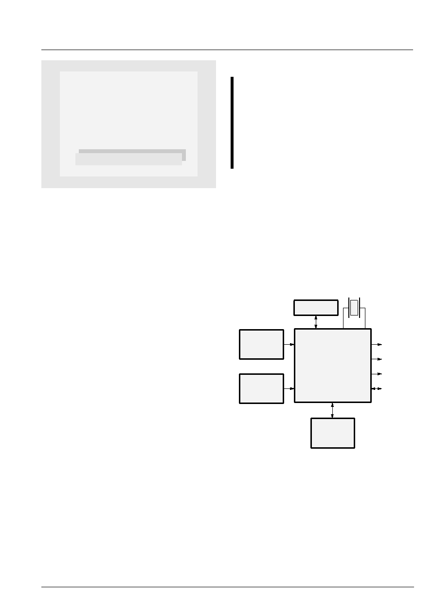
The field of applications covers analog and digital TV
sets, set-top satellite decoders, video recorders and
home computers. For example, Fig. 2–4 shows how the
TPU 3040 fits into an analog environment. Two analog
sources are connected and the output is analog RGB,
synchronized with an external sync signal or self-timed.
Page selection and other user actions are sent to the
TPU 3040 via I2C-Bus using a high level command lan-
guage.
Tuner 1
Tuner 2
DRAM
R
G
B
Sync
I2C-Bus
TPU 3040
Fig. 2–4: Stand-Alone Application
Controller
相關(guān)PDF資料 |
PDF描述 |
|---|---|
| TPU3035PO | TELETEXT DECODER, PDIP52 |
| TPU3035PQ | TELETEXT DECODER, PQCC44 |
| TPU3050PK | TELETEXT DECODER, PDIP40 |
| TPU3050PO | TELETEXT DECODER, PDIP52 |
| TPU3050PQ | TELETEXT DECODER, PQCC44 |
相關(guān)代理商/技術(shù)參數(shù) |
參數(shù)描述 |
|---|---|
| TPU304 | 制造商:未知廠家 制造商全稱:未知廠家 功能描述:TRANSISTOR | JFET | P-CHANNEL | 30MA I(DSS) | TO-226AA |
| TPU3040 | 制造商:MICRONAS 制造商全稱:MICRONAS 功能描述:Teletext Processors |
| TPU3040(DIP40) | 制造商:未知廠家 制造商全稱:未知廠家 功能描述:Teletext Circuit |
| TPU3040(PDIP40) | 制造商:未知廠家 制造商全稱:未知廠家 功能描述:Microprocessor |
| TPU3040(PSDIP52) | 制造商:未知廠家 制造商全稱:未知廠家 功能描述:Microprocessor |
發(fā)布緊急采購(gòu),3分鐘左右您將得到回復(fù)。